Spread spectrum controllable delay clock buffer with zero cycle slip

a delay clock and controllable technology, applied in the direction of transmission, electrical equipment, phase difference detection, etc., can solve the problem that devices provide no benefit in emi reduction

Active Publication Date: 2010-03-09
SEMICON COMPONENTS IND LLC
View PDF13 Cites 10 Cited by
  • Summary
  • Abstract
  • Description
  • Claims
  • Application Information

AI Technical Summary

Benefits of technology

[0010]The present invention generally comprises a controllable delay clock buffer that provides spread spectrum modulation of the output signals with zero cycle slip. In one aspect, the invention provides a controllable delay buffer in which a PLL is connected to a PLL loop filter, and the SS modulation frequency is injected into the PLL loop filter. A typical loop filter is an RC series network connected to ground, and the signal may be a controlled current injected into the capacitor of the loop filter. This technique enables the application of spread spectrum modulation to a PWM system with a minimum number of additional components.

Problems solved by technology

Conventional controllable delay buffers have both input and output clocks without spread spectrum modulation, but these devices provide no benefit in EMI reduction.

Method used


Image

  • Spread spectrum controllable delay clock buffer with zero cycle slip
  • Spread spectrum controllable delay clock buffer with zero cycle slip
  • Spread spectrum controllable delay clock buffer with zero cycle slip

Examples


example # 1

Example #1

±∂=±1%=± 1 / 100

FCLK=100 MHz

FMR=100 KHz

[0045]

example # 2

Example #2

±∂=±0.1%=± 1 / 1000

FCLK=100 MHz

FMR=100 KHz

[0046]

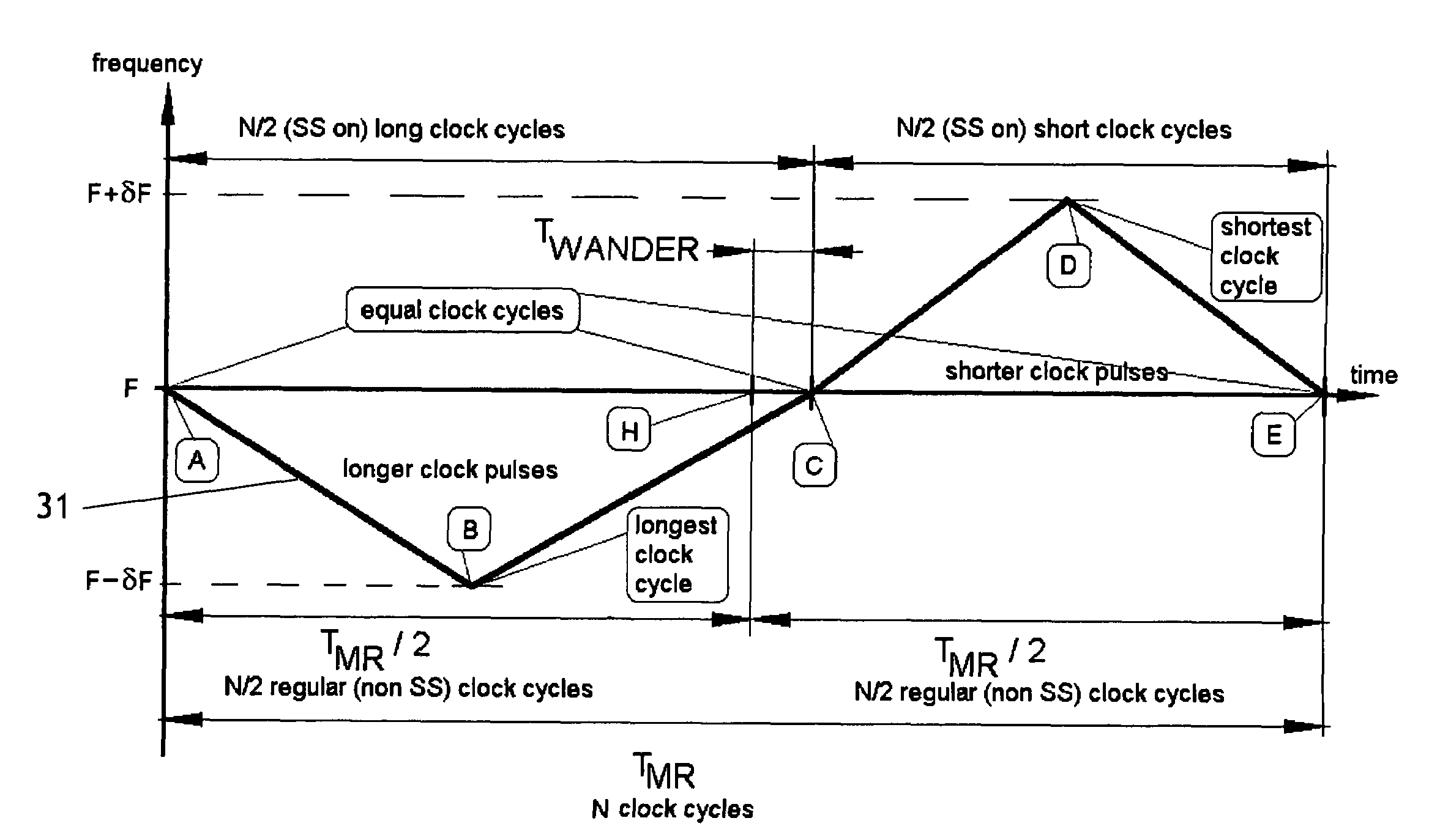
[0047]Thus it is clear that if the peak frequency deviation does not exceed a computable limit, there will be no cycle slip. Indeed, given that the peak frequency deviation is a function of the SS modulation signal, it is possible to design a device in accordance with this invention that is guaranteed to produce a SS output signal having zero cycle slip. This is a significant advantage for use as a clock signal generator that provides SS modulation to defeat EMI noise spikes that would otherwise be caused by a constant frequency clock signal.

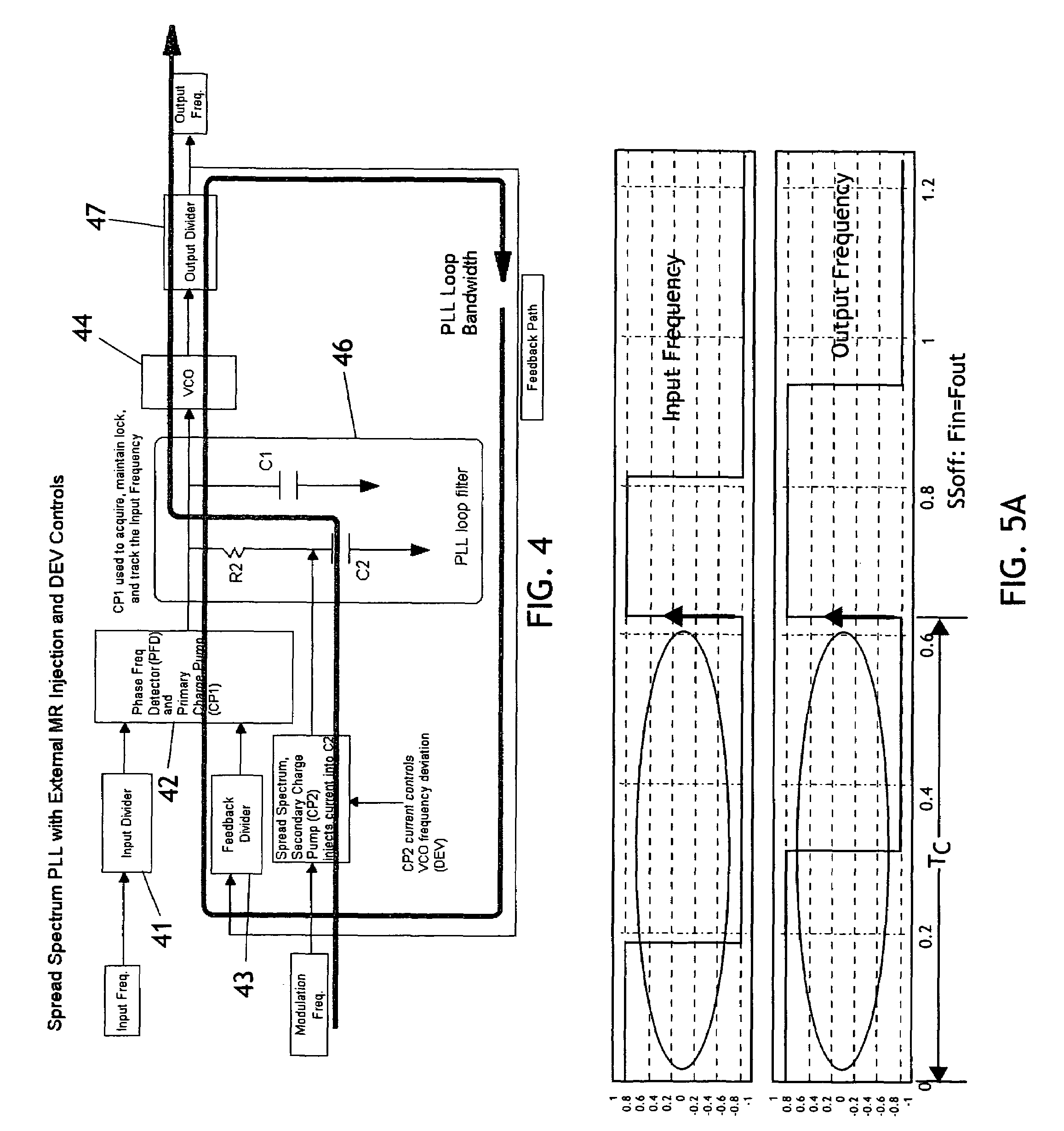
[0048]With reference to FIG. 8, it is noted that the SS modulation method of the invention exhibits another interesting and useful trait. The PLL loop bandwidth lowpass profile extends from zero frequency to the BWmax point at the upper end of the loop bandwidth. (This frequency is actually much lower than the maximum input / output frequencies of the PLL loop itself.) The SS modulation signa...


PUM


Abstract

A controllable delay clock buffer that provides spread spectrum modulation of the output signals with zero cycle slip includes a PLL having a PLL loop filter that comprises an RC network. A clock signal is input to the PLL, and a SS modulation frequency is injected into the capacitor of the PLL loop filter. The SS signal is provided by a secondary charge pump that produces a programmable waveform such as a square wave or a stair case square wave current signal. The programmable waveform is integrated by the loop filter capacitor to form a corresponding triangular or trigonal waveform which varies the input to the VCO of the PLL to define a frequency modulation profile that has a corresponding triangular or trigonal envelope. The bandpass profile of the SS modulation signal is at a higher frequency range than the lowpass profile of the PLL, so that the SS waveform profile is not distorted or cancelled by the PLL.

Description

CROSS-REFERENCE TO RELATED APPLICATIONS[0001]Not applicable.FEDERALLY SPONSORED RESEARCH[0002]Not applicable.SEQUENCE LISTING, ETC ON CD[0003]Not applicable.BACKGROUND OF THE INVENTION[0004]1. Field of the Invention[0005]This invention relates to a controllable delay clock buffer and, more particularly, to a controllable delay clock buffer that provides spread spectrum modulation of the clock signal and zero cycle slip.[0006]2. Description of Related Art[0007]A controllable delay buffer is a device that accepts an input signal (typically a periodic clock signal) and provides an output that has its transition edges phase aligned (controlled) with respect to those of the input signal. The definition of a transition edge is a change in voltage or current from one stable state to another. Phase alignment implies that the measured phase (time) difference between the 2 edges of the input and output is less than a certain specified value.[0008]Controllable delay clock buffers are typically...

Claims


Application Information

Patent Timeline
Patent Type & Authority Patents(United States)
IPC IPC(8): H03D3/24
CPCH03B23/00
Inventor VENUGOPAL, NARENDARHARITON, DAN I.MANDAL, DIPANKARKUMAR, SUSHILHOEFT, WERNER
Owner SEMICON COMPONENTS IND LLC
Why Eureka
Try Eureka