Supercharge Your Innovation With Domain-Expert AI Agents!

Electronic device and manufacturing method of the same

a manufacturing method and technology of electronic components, applied in the direction of printed circuit manufacturing, coupling device connection, printed circuit aspects, etc., can solve the problems of difficult to ensure co-planarity in connection portions between terminals and lands, the probability of positional shift between a terminal and a land or the falling of the terminal from the land, and the inability to improve the packaging density of the electronic component without difficulty, so as to improve the connection reliability between the electronic element and the printed circuit board. ,

Inactive Publication Date: 2010-03-16
DENSO CORP
View PDF25 Cites 10 Cited by
  • Summary
  • Abstract
  • Description
  • Claims
  • Application Information

AI Technical Summary

Benefits of technology

This approach improves connection reliability and packaging density by eliminating the need for flow soldering, reducing positional shifts, and minimizing voids, while maintaining a robust connection between terminals and lands.

Problems solved by technology

That is, as the area in which electronic-component mounting is disabled is large, the electronic component packaging density cannot be improved without difficulty in the whole (both surfaces) of the printed circuit board.
For example, upon reflow process, when deformation (warp or the like) occurs in the printed circuit board (housing of the electronic component) due to a difference between linear expansion coefficients of the printed circuit board and the electronic component, there is a probability of positional shift between a terminal and a land or falling of the terminal from the land.
Further, in accordance with increase in the number of terminals, it becomes difficult to ensure co-planarity in connection portions between the terminals and the lands.
Further, it is further difficult to ensure connection all the terminals and corresponding lands due to the influence of warp of the printed circuit board or the like.
That is, this structure has a problem in the point of connection reliability.
Further, the amount of positional shift with the insertion member as a rotational axis is large.
Further, voids (bubbles) might be formed in the solder flowed in the through hole.
Also, the electronic component packaging density cannot be improved without difficulty.
However, according to JP-11-317265A and JP-7-153508A, a terminal connected with a land positioned away from the main body disturbs supply of reflowing heat to a terminal connected with a land positioned closer to the main body (junction with the land) than the above land.
Accordingly, upon reflowing, the terminal connected with the land positioned away from the main body blocks heat to the terminal connected with the land closer to the main body, and connection reliability may be lowered in the junction (soldering failure may occur).

Method used


Image

  • Electronic device and manufacturing method of the same
  • Electronic device and manufacturing method of the same
  • Electronic device and manufacturing method of the same

Examples


first embodiment

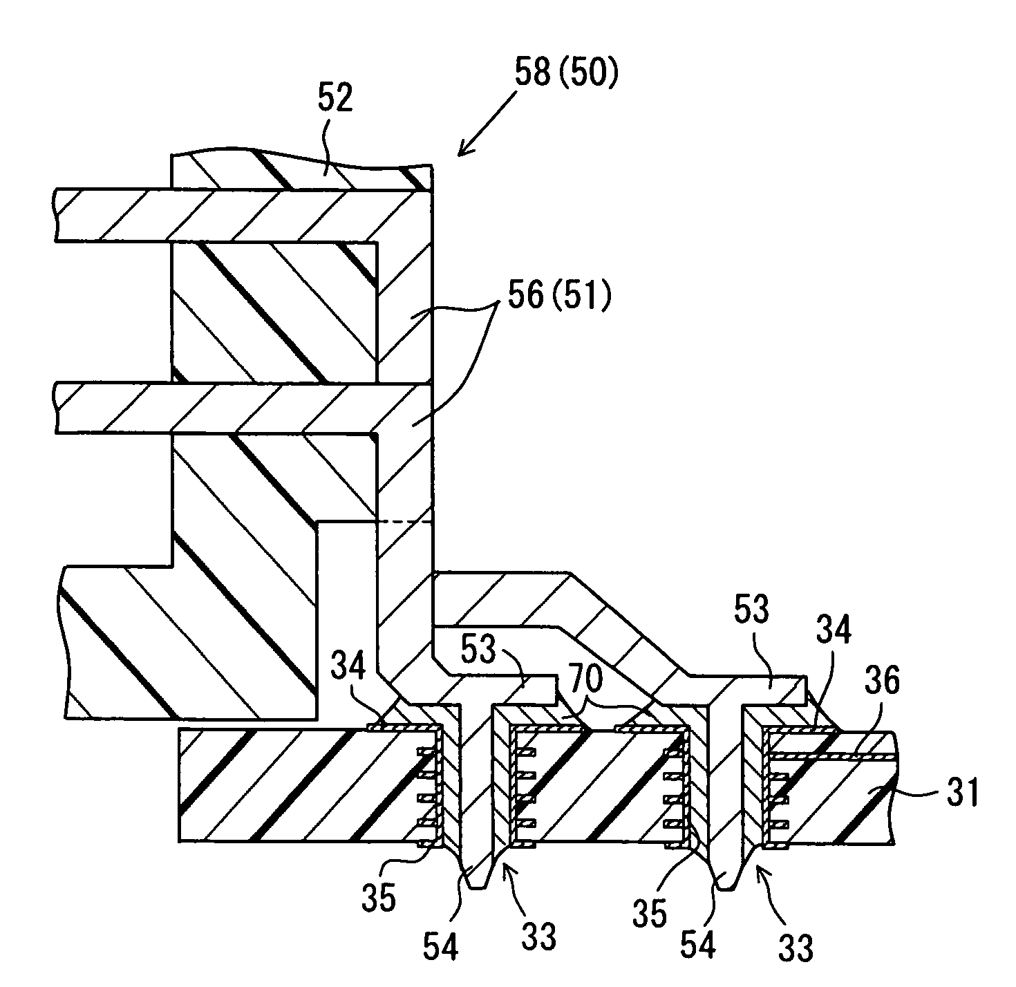
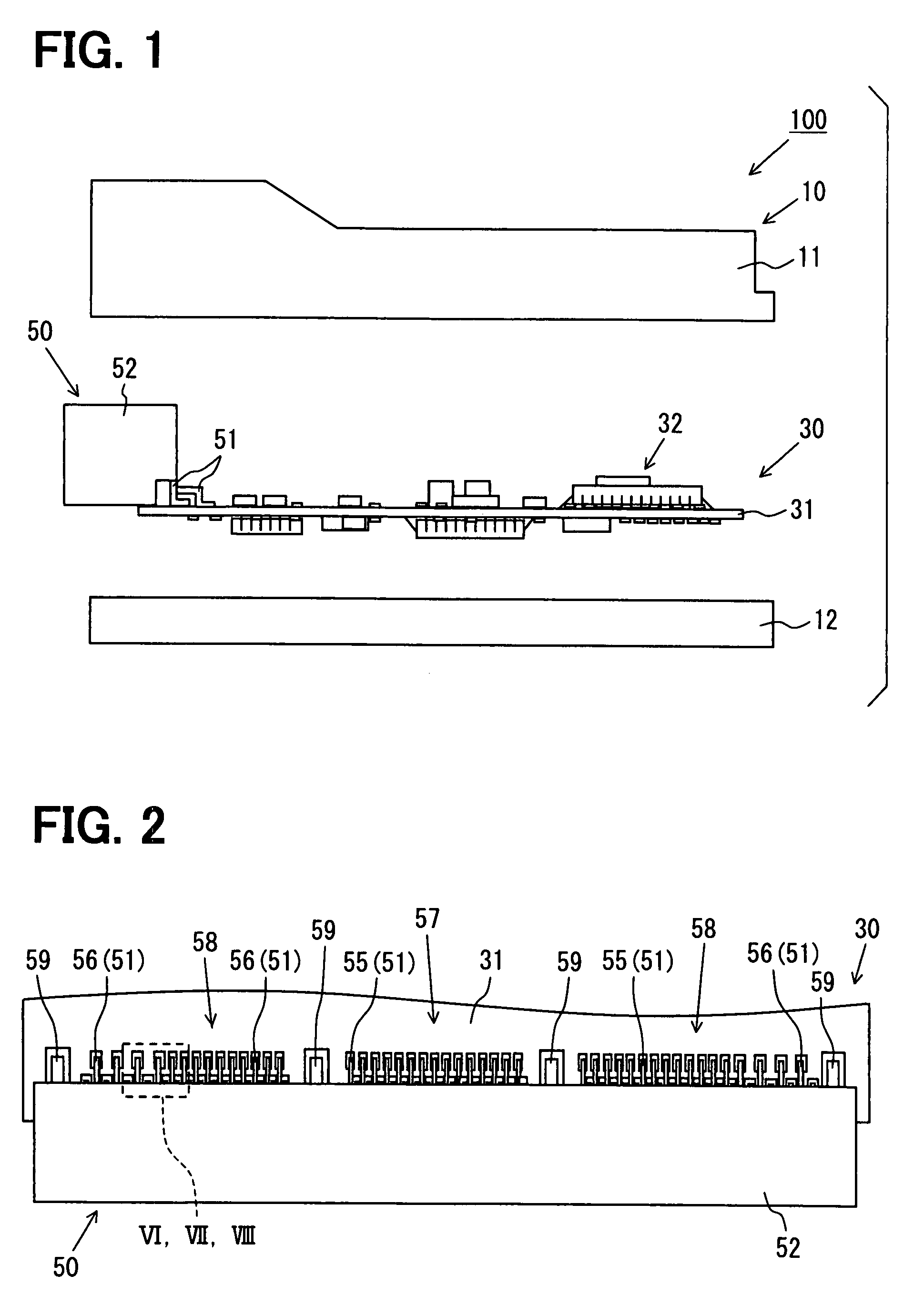
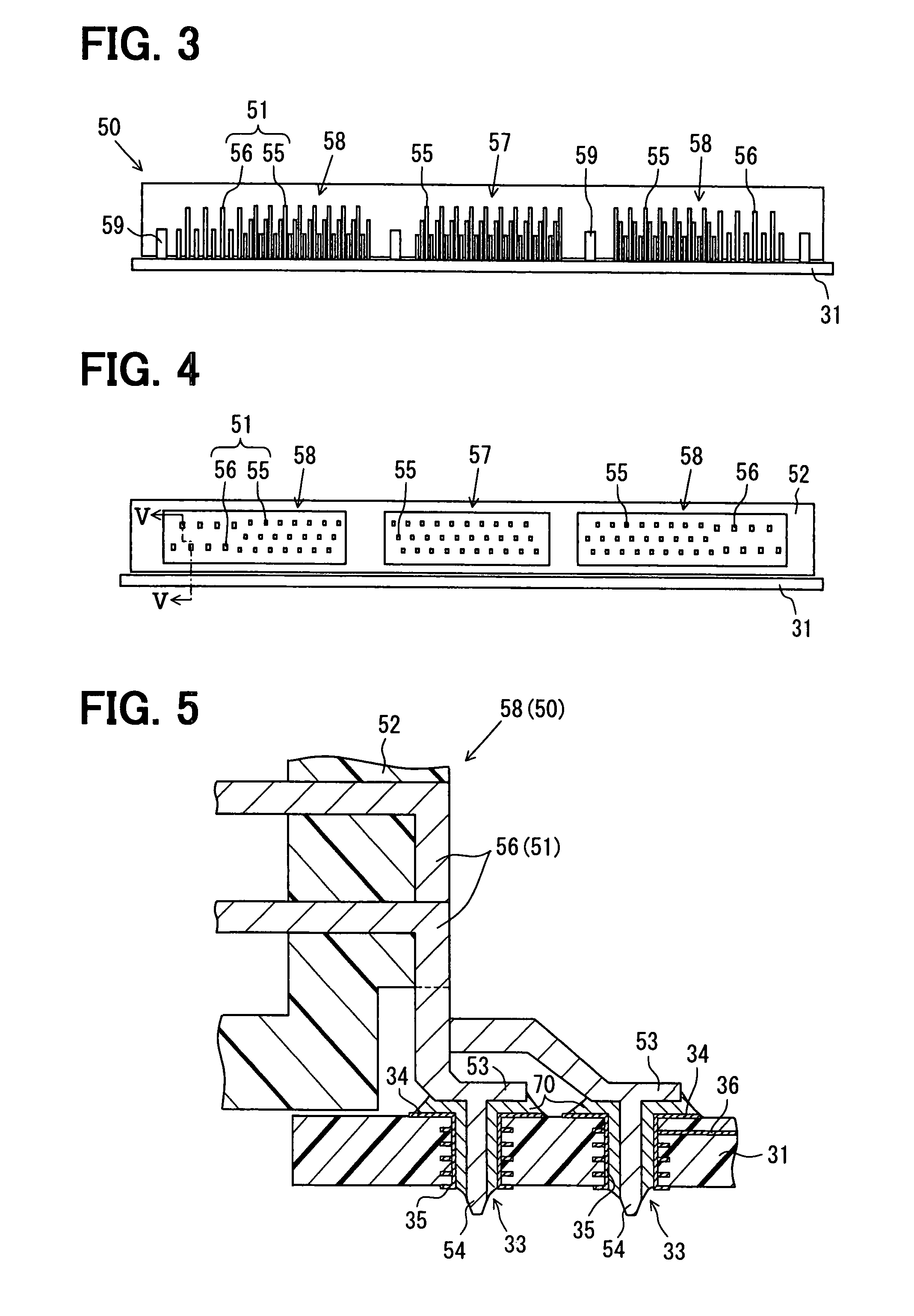
[0102]FIG. 1 is an exploded diagram showing a pre-assembly status for explanation of the schematic structure of an electronic control device according to a first embodiment. FIG. 2 is a plan view of a peripheral portion of a connector mounted on a printed circuit board. FIG. 3 is a plan view of the connector mounted on the printed circuit board viewed from the side of connection between the printed circuit board and terminals. FIG. 4 is a plan view of the connector mounted on the printed circuit board viewed from the side of connection between the printed circuit board and external connectors. FIG. 5 is a cross-sectional view along a line V-V in FIG. 4. FIG. 6 is an expanded plan view of an area indicated with a broken line in FIG. 2 on the side of an electronic component mounting surface. FIG. 7 is an expanded plan view of the electronic component mounting surface of the printed circuit board in the area indicated with the broken line in FIG. 2. FIG. 8 is an expanded plan view of t...

second embodiment

[0152]Next, a second embodiment of the present invention will be described based on FIGS. 24 and 25. FIG. 24 is an expanded cross-sectional view of a peripheral portion of the connector mounted on the printed circuit board, for explanation of the concept in the structure shown in the first embodiment. FIG. 25 is an expanded cross-sectional view of the peripheral portion of the connector mounted on the printed circuit board in the electronic control device according to the second embodiment.

[0153]The electronic control device and its manufacturing method according to the second embodiment have many commonalities with those in the first embodiment, accordingly, the detailed explanations of such commonalities will be omitted, and the difference will be mainly described. Further, in the present embodiment, constituent elements identical to those in the first embodiment have the same reference numerals.

[0154]In the first embodiment, the insertion member 54 of the branch terminal 51 is pr...

third embodiment

[0161]Next, a third embodiment of the present invention will be described based on FIG. 28. FIG. 28 is a plan view of a peripheral portion of the connector mounted on the printed circuit board in the electronic control device according to the third embodiment.

[0162]As the electronic control device 100 and its manufacturing method according to the third embodiment have many commonalities with those in the first embodiment, the detailed explanations of such commonalities will be omitted hereinbelow, but the difference will be mainly described. Further, in the present embodiment, constituent elements identical to those in the first embodiment have the same reference numerals.

[0163]In the first embodiment, all the terminals which provide an electrical connection function are the branch terminals 51. On the other hand, in the present embodiment, as shown in FIG. 28, the connector 50 includes a surface mounting type terminal 60 as a terminal to provide an electrical connection function, i...


PUM


Abstract

An electronic device includes a printed circuit board with multiple lands and through holes and an electronic element with multiple terminals on the board. Each terminal is coupled with the land through a solder. The lands include a surface land on the board and an insertion land on a sidewall of the through hole. The terminals include a branch terminal having an insertion member and a surface member. The insertion member is coupled with the insertion land through the solder. The surface member is coupled with the surface land through the solder. The surface member is parallel to the printed circuit board. The insertion member is perpendicular to the printed circuit board. The insertion member extends from a part of the surface member, which faces the surface land and disposed above the through hole.

Description

CROSS REFERENCE TO RELATED APPLICATIONS[0001]This application is based on Japanese Patent Applications No. 2006-232602 filed on Aug. 29, 2006, No. 2006-336153 filed on Dec. 13, 2006, No. 2007-888 filed on Jan. 8, 2007, No. 2007-35330 filed on Feb. 15, 2007 and No. 2007-148613 filed on Jun. 4, 2007, the disclosures of which are incorporated herein by reference. This application is also related to U.S. application Ser. No. 11 / 979,972, entitled “ELECTRONIC DEVICE,” filed simultaneously on Nov. 13, 2007 with the present application.FIELD OF THE INVENTION[0002]The present invention relates to an electronic device and a method for manufacturing an electronic device.BACKGROUND OF THE INVENTION[0003]Conventionally, as an electronic device manufactured by mounting electronic components such as a connector on a printed circuit board, a device having an insertion-mounting structure is known. In this structure, a terminal of an electronic component is inserted in a through hole of a printed cir...

Claims


Application Information

Patent Timeline
Patent Type & Authority Patents(United States)
IPC IPC(8): H01R12/00
CPCH01R43/0256H05K1/023H05K1/116H05K3/3405H05K3/3447H05K3/3484H05K2201/09381H05K2201/094H05K2201/09709H05K2201/09727H05K2201/0979H05K2201/10189H05K2201/10446H05K2201/10757H05K2201/10787H05K2201/10803H05K2201/10871H05K2201/10901H05K2203/1178H05K2203/1394H01R12/707H05K3/3485
Inventor HONDA, TAKAYOSHI
Owner DENSO CORP
Features
  • R&D
  • Intellectual Property
  • Life Sciences
  • Materials
  • Tech Scout
  • Unparalleled Data Quality
  • Higher Quality Content
  • 60% Fewer Hallucinations
Learn More