Process for manufacturing a membrane of semiconductor material integrated in, and electrically insulated from, a substrate

a manufacturing process and semiconductor material technology, applied in the direction of microstructured devices, microstructured technology, instruments, etc., can solve the problems of insufficient electrical or thermal insulation of the membrane thus obtained, the implementation of the above-mentioned techniques is in general complex, and the cost of manufacturing is considerabl

Active Publication Date: 2010-03-16
STMICROELECTRONICS SRL
View PDF3 Cites 26 Cited by
  • Summary
  • Abstract
  • Description
  • Claims
  • Application Information

AI Technical Summary

Benefits of technology

[0017]In accordance with another aspect of the foregoing embodiment, the trench is formed away from the membrane and anchorages of the membrane to the substrate a distance of separation to prevent mechanical stresses on the membrane due to discontinuity represented by a silicon-oxide junction created by the insulation structure.

Problems solved by technology

The aforesaid techniques are in general complex to implement and involve considerable manufacturing costs.
However, the problem of electrical or thermal insulation of the membrane thus obtained has not yet been adequately solved, so that this manufacturing process is not currently completely exploitable in applications in which the insulation of the membrane from the substrate from which it is obtained is required.

Method used


Image

  • Process for manufacturing a membrane of semiconductor material integrated in, and electrically insulated from, a substrate
  • Process for manufacturing a membrane of semiconductor material integrated in, and electrically insulated from, a substrate
  • Process for manufacturing a membrane of semiconductor material integrated in, and electrically insulated from, a substrate

Examples


second embodiment

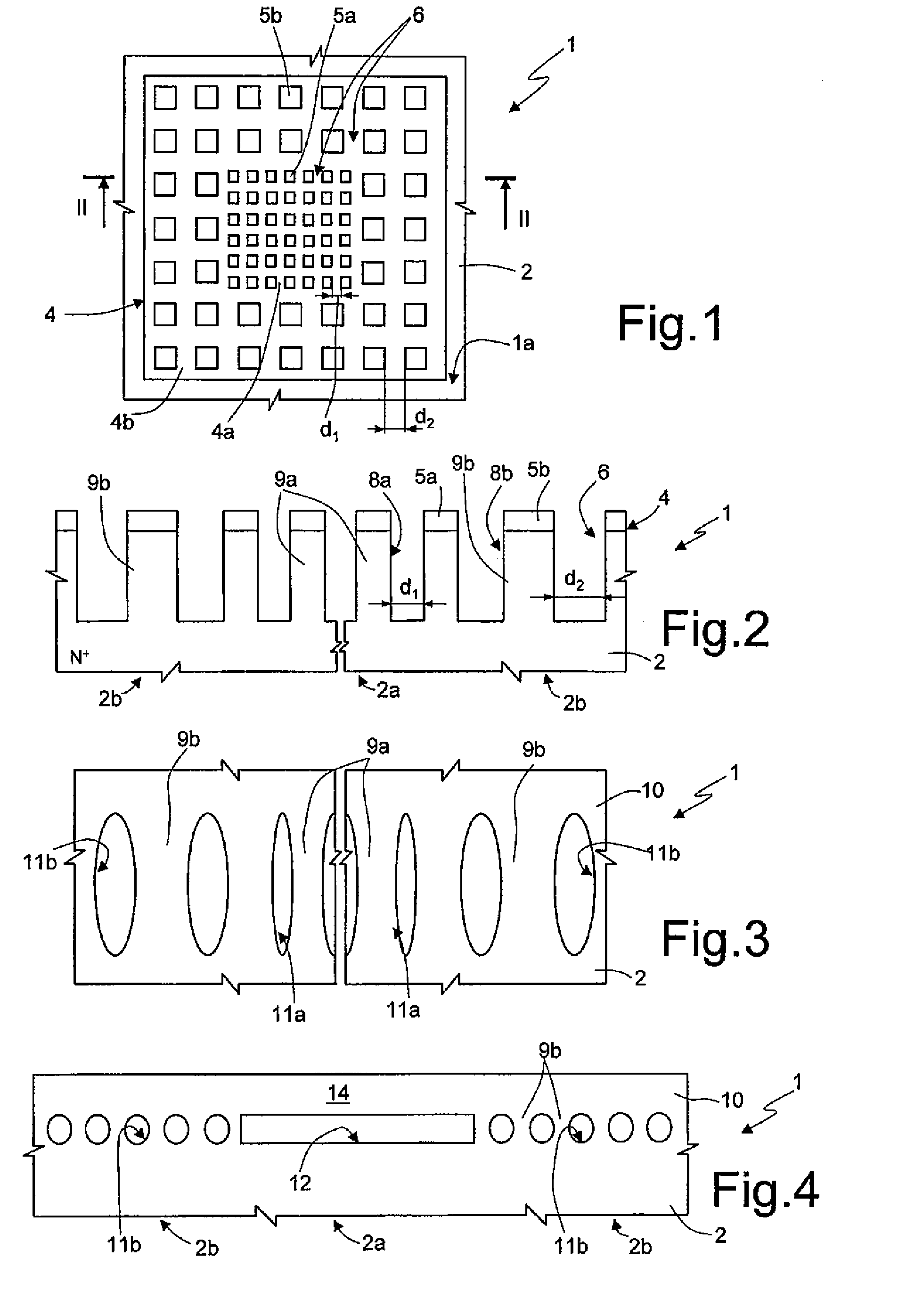
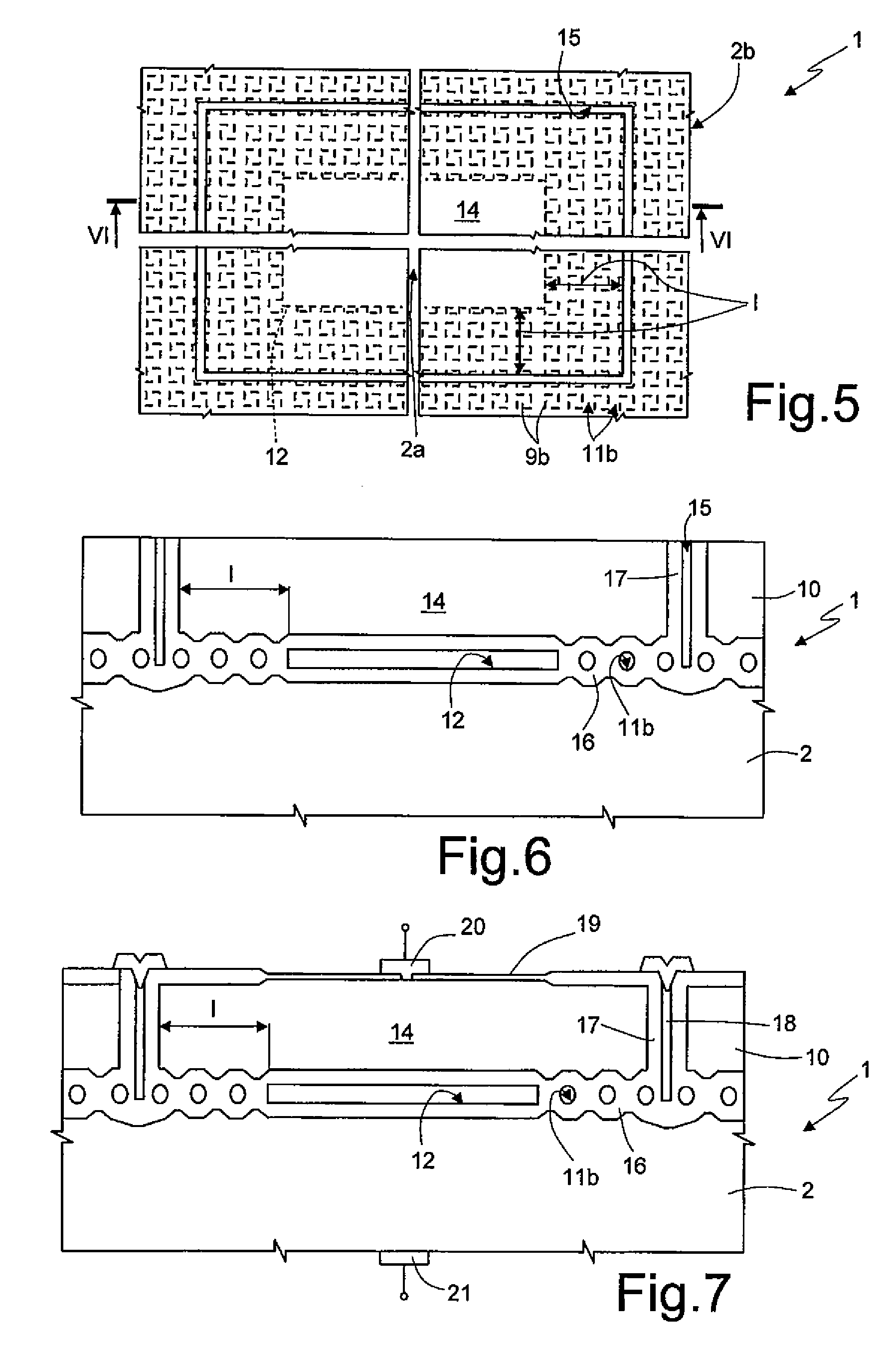
[0040]the present disclosure envisages a different process for formation of the vertical insulation region; also in this case, process steps are carried out such that this region is set outside the membrane 14, at a certain distance of separation I, so as to prevent any mechanical stresses therein.

[0041]In detail, the process envisages (FIG. 8) formation of the buried cavity 12 within the substrate 2 and the membrane 14, as described previously. It is to be noted that, in this case, the buried insulation region is not formed at the side of the cavity 12 (basically, just the first mask region 4a is used for formation of the first columns 9a at the first separation distance d1). On the top surface 1a of the wafer a resist layer is then formed, which is appropriately defined so as to form an etching mask 24.

[0042]Next (FIGS. 9a-9c), through the etching mask 24, an external peripheral portion of the membrane 14 is etched, and a plurality of trenches 25 are opened, each of which extends ...

first embodiment

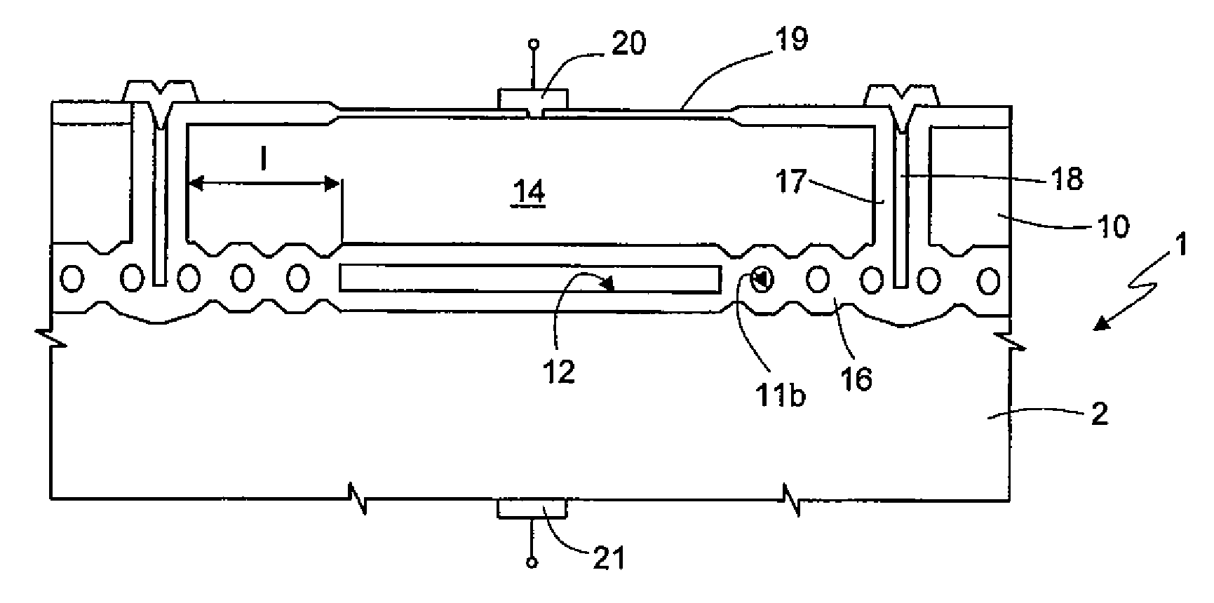
[0053]In particular, in the first embodiment, the buried insulation region 16 can be confined to just the sensor (hence surrounding only the membrane 14), or else can extend throughout a silicon die, as far as the scribing lines in which cutting of the wafer 1 is performed.

[0054]Furthermore, the structure of the mask 4 and the shape of the deep trenches 8a, 8b and of the columns 9a, 9b can vary with respect to what is illustrated herein. For example, the mask 4 can have a structure complimentary to the one described previously, and consequently including a grid-shaped structure defining a plurality of openings of a polygonal shape, or else the same mask can be shaped like a grating to define openings having a striplike shape. The same columns 9a, 9b can also have a different shape (for example, with hexagonal cross section).


PUM


Abstract

A process for manufacturing an integrated membrane made of semiconductor material includes the step of forming, in a monolithic body of semiconductor material having a front face, a buried cavity, extending at a distance from the front face and delimiting with the front face a surface region of the monolithic body, the surface region forming a membrane that is suspended above the buried cavity. The process further envisages the step of forming an insulation structure in a surface portion of the monolithic body to electrically insulate the membrane from the monolithic body; and the further and distinct step of setting the insulation structure at a distance from the membrane so that it will be positioned outside the membrane at a non-zero distance of separation.

Description

BACKGROUND[0001]1. Technical Field[0002]The present disclosure relates to a process for manufacturing a membrane made of semiconductor material that is integrated in, and electrically insulated from, a substrate.[0003]2. Description of the Related Art[0004]A large number of integrated semiconductor sensors are known, made with micromachining techniques, which base their operation on detection of a deformation of a thin membrane (also defined as diaphragm), suspended above a cavity. Among these sensors it is possible, for example, to mention absolute or differential, capacitive or piezoresistive, pressure sensors, inertial sensors, chemical sensors, magnetic-field sensors, and microphones. It is also known that it is often advantageous, or even necessary, to provide an electrical, and possibly thermal, insulation of the membrane.[0005]Main known techniques for manufacturing electrically insulated membranes envisage the use of a SOI (Silicon On Insulator) wafer, or of surface micromac...

Claims


Application Information

Patent Timeline
Patent Type & Authority Patents(United States)
IPC IPC(8): H01L21/00
CPCB81C1/00158B81C2201/0116
Inventor VILLA, FLAVIO FRANCESCOCORONA, PIETROCOMBI, CHANTALBALDO, LORENZOBARLOCCHI, GABRIELE
Owner STMICROELECTRONICS SRL
Why Eureka
Try Eureka