System and method for voltage noise and jitter measurement using time-resolved emission

a technology of time-resolved emission and voltage noise, which is applied in the direction of noise figure or signal-to-noise ratio measurement, instruments, testing vessel construction, etc., can solve the problems of affecting the electrical behavior of the circuit, and affecting the performance of many high-speed circuits

Active Publication Date: 2010-03-16
DCG SYST
View PDF8 Cites 9 Cited by
  • Summary
  • Abstract
  • Description
  • Claims
  • Application Information

AI Technical Summary

Problems solved by technology

Circuit jitter limits the performance of many high-speed circuits.
It also limits the clock frequency of microprocessors, advanced chipsets, graphics processors, and other circuits relying on phase-locked loops (PLLs) and clock distribution networks.
While such measurement enable real-time measurements of jitter timing, the mechanical probing process can load a circuit so much that it alters the electrical behavior of the circuit.
The source of timing jitter is local voltage noise.
On the other hand, deterministic, synchronous jitter causes a variation in the timing delay between TRE peaks, but not broadening of the peaks.

Method used


Image

  • System and method for voltage noise and jitter measurement using time-resolved emission
  • System and method for voltage noise and jitter measurement using time-resolved emission
  • System and method for voltage noise and jitter measurement using time-resolved emission

Examples


Embodiment Construction

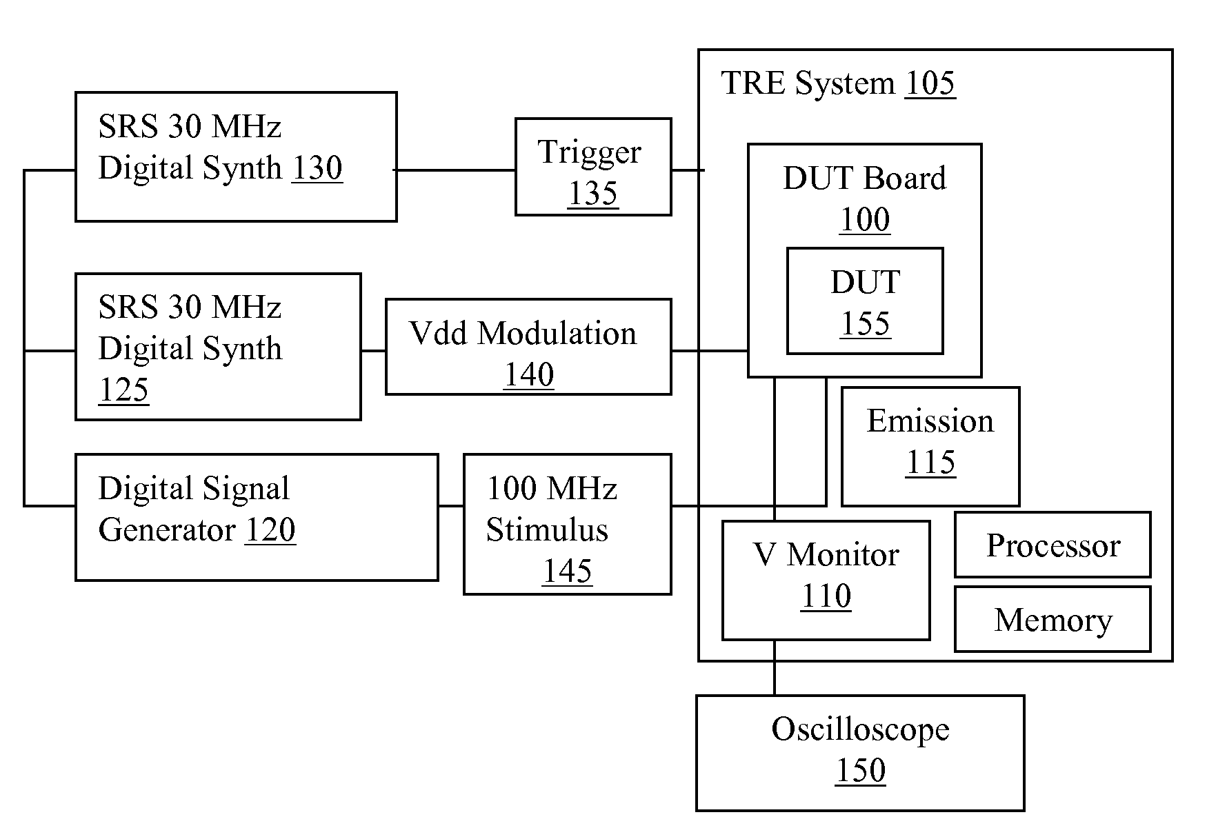
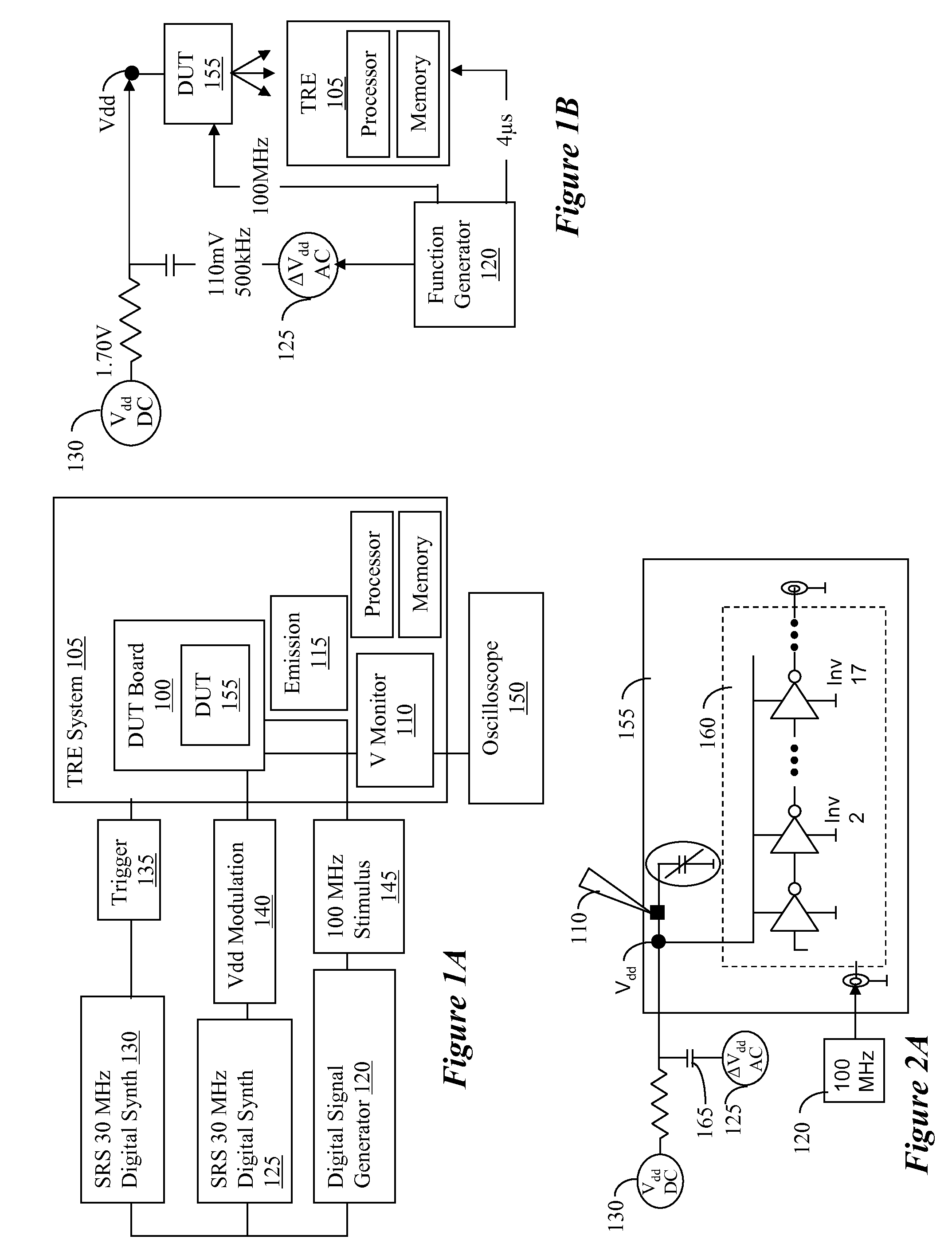
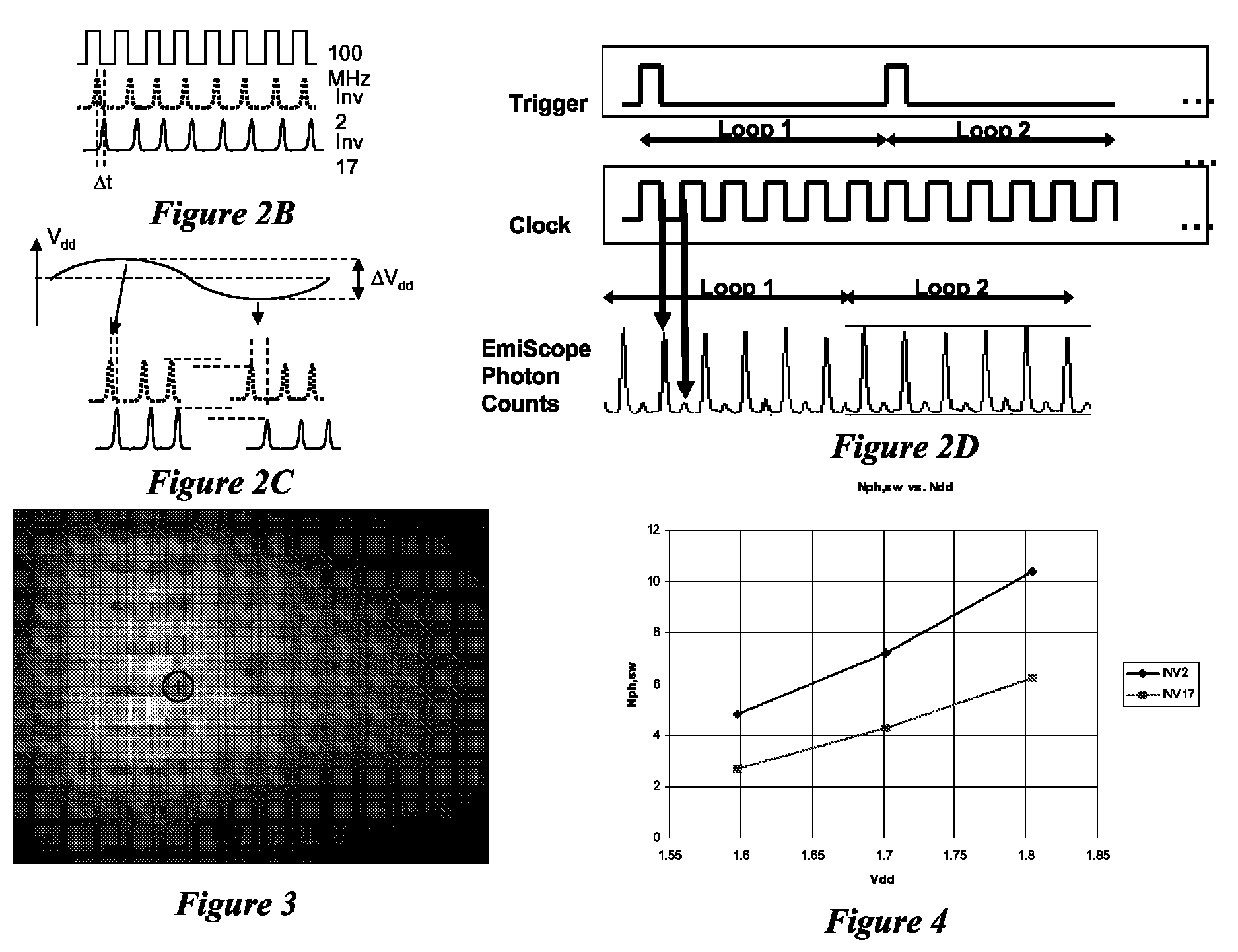
[0037]The following is a detailed description of embodiments of the invention for measuring deterministic jitter and the local voltage variation causing it. One aspect of the invention is the use of a TRE system (or other non-invasive timing tool, such as the IDS 2000 / 2500 from Credence) to acquire transition events from an integrated circuit and apply new methodologies to the acquired signal to obtain the new measurements. According to embodiments of the invention, the device under test (DUT) is stimulated repeatedly by repeating a test loop a statistically significant number of times. The test loop can be provided by a tester or some other stimulus system capable of providing repeated stimulus loops. The response of a specific device to the stimulus is measured non-invasively, such as by photon emission system, laser tester, RF modulation, or the likes. The obtained signal is fitted into mathematical curve, such as Gaussian curves, so as to generate peaks corresponding to the stim...


PUM


Abstract

Time-resolved emission can be used to measure loop-synchronous, small-signal voltage perturbation in integrated circuits. In this technique the measurements are completely non-invasive and so reflect the true device behavior. The time-dependant propagation delay caused by Vdd modulation also shows the expected qualitative signature. This technique should find applications in circuits with relatively fast clock-like circuits where loop-synchronous voltage pickup is limiting circuit behavior.

Description

RELATED APPLICATIONS[0001]This application claims priority from Provisional Application Ser. No. 60 / 744,329, filed Apr. 5, 2006, the entire content thereof is incorporated herein by reference.BACKGROUND[0002]1. Field of the Invention[0003]This invention relates to time-resolved emission for timing and voltage measurement. More specifically, this invention relates to using time-resolved emission to measure timing perturbation and voltage modulation signals inside an integrated circuit.[0004]2. Description of Related Art[0005]Time-resolved emission (TRE) is commonly used for circuit debug and advanced timing-related failure analysis. Established application areas include localization of resistive interconnects, timing contention, circuit debug, clock distribution skew analysis, and other timing-related fault isolation techniques.[0006]The basic concepts of time-resolved emission have been covered extensively in the prior art. The carriers responsible for the source-drain current in a ...

Claims


Application Information

Patent Timeline
Patent Type & Authority Patents(United States)
IPC IPC(8): G01R31/16
CPCG01R29/26G01R31/2882G01R31/311G01R31/31709G01R31/31725
Inventor KASAPI, STEVENWOODS, GARY LEONARD
Owner DCG SYST
Why Eureka
Try Eureka