Continuous wave based bias method and apparatus for minimizing MOS transistor distortion

a technology of metaloxidesemiconductor transistor and bias method, which is applied in the direction of amplifiers, amplifiers with semiconductor devices/discharge tubes, amplifiers, etc., can solve the problems of circuit layout problems and design circuits with sufficient linearity performance, and achieve the effect of minimizing distortion in transistor circuits

Active Publication Date: 2010-03-16
MAXLINEAR ASIA SINGAPORE PTE LTD
View PDF8 Cites 36 Cited by
  • Summary
  • Abstract
  • Description
  • Claims
  • Application Information

AI Technical Summary

Benefits of technology

[0007]It is an object of the present invention to obviate or mitigate at least one disadvantage of previous biasing schemes for minimizing distortion in transistor circuits.

Problems solved by technology

Put simply, designing a circuit with sufficient linearity performance is often one of the greatest challenges in RF design.
The large number of components required in making such biasing circuits and the fact that space available on a circuit die is usually quite limited, can lead to circuit layout problems.

Method used


Image

  • Continuous wave based bias method and apparatus for minimizing MOS transistor distortion
  • Continuous wave based bias method and apparatus for minimizing MOS transistor distortion
  • Continuous wave based bias method and apparatus for minimizing MOS transistor distortion

Examples


Embodiment Construction

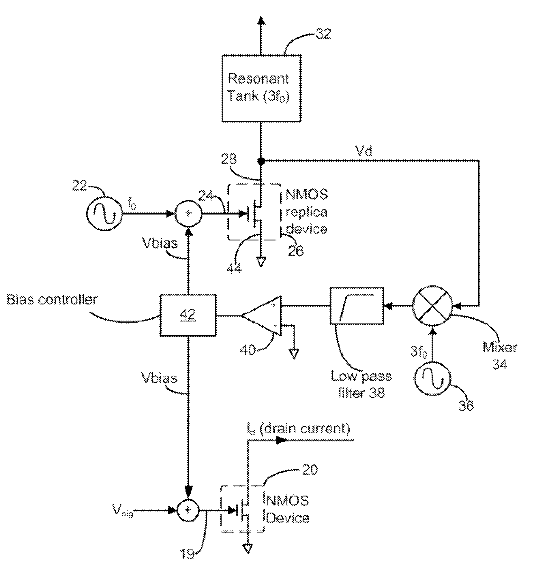
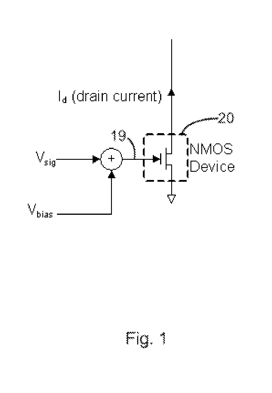
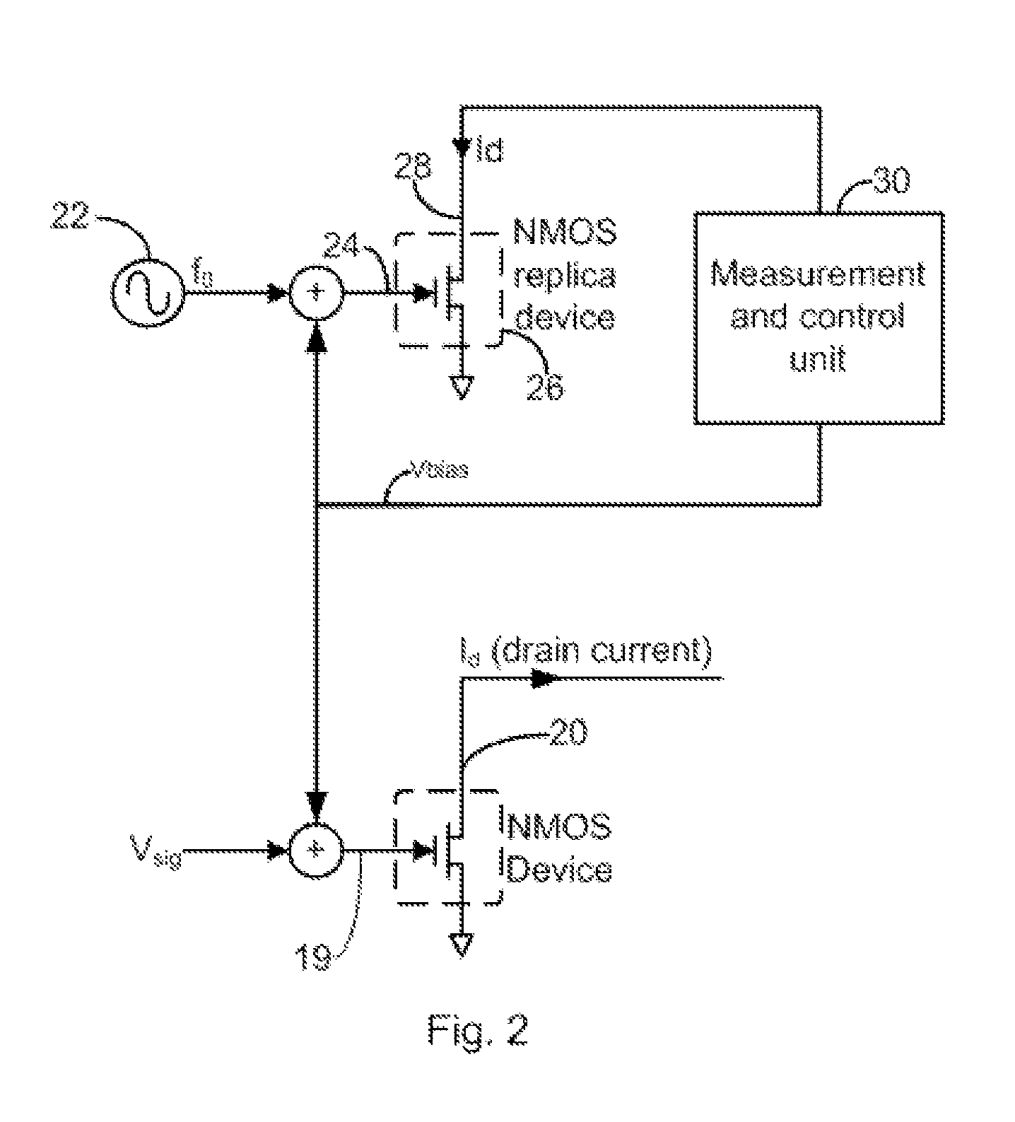
[0020]Generally, the present invention provides a method and biasing circuit for minimizing Nth-order distortion in a first transistor circuit by adjusting the bias at the input of the first transistor circuit. A first CW signal having a fixed frequency fo is provided at the input of a replica transistor circuit of the first transistor circuit to obtain an output signal at the output of the replica transistor circuit. The output signal is mixed with another CW signal having a frequency equal to N*fo. The resulting mixed signal includes a DC component having an intensity proportional to the Nth-order distortion present in the output signal. A feedback circuit adjusts the bias at the input of the replica transistor circuit, and at the input of the first transistor circuit, to minimize the DC component of the mixed signal.

[0021]The following describes embodiments of the invention for metal-oxide-semiconductor transistors; however, as will be understood by the worker skilled in the art,...


PUM


Abstract

A biasing circuit and method for minimizing distortion in a MOS transistor. A first CW source provides a first CW signal at the input of a replica transistor to obtain an output signal at the output of the replica transistor. The output signal is mixed with another CW signal having a frequency equal to N times that of the first CW signal, N being an integer greater than one, to obtain a mixed signal having a DC component with an intensity proportional to the Nth-order distortion present in the output signal. A bias voltage to minimize this distortion is then applied to the input of the original transistor on which the replica transistor is based, the bias voltage determined in accordance with the intensity of the DC component.

Description

FIELD OF THE INVENTION[0001]The present invention relates generally to transistor circuits. More particularly, the present invention relates to the control of distortion in metal-oxide-semiconductor transistor circuits.BACKGROUND OF THE INVENTION[0002]Transistor amplifiers are commonly used building blocks of analog circuits operating at frequencies ranging from audio to radio frequencies (RF). Generally, these circuits are required to produce minimal distortion of the signal they operate on to preserve information carried by the signal. In circuits that implement feedback, a designer has the option to reduce distortion by controlling the loop gain of the circuit at the expense of overall gain. In feed-forward circuits however, other means of improving linearity, i.e., reducing distortion, are required.[0003]As an example, RF circuits are a common application in which one faces these issues. An RF designer is typically compelled to use feed-forward architectures due to the high freq...

Claims


Application Information

Patent Timeline
Patent Type & Authority Patents(United States)
IPC IPC(8): H03G3/10
CPCH03F1/301H03F1/3205H03F2200/18H03F2200/453
Inventor MCADAM, MATTHEW W.BEAUDOIN, FRANCIS
Owner MAXLINEAR ASIA SINGAPORE PTE LTD
Why Eureka
Try Eureka