
Power amplifier

a power amplifier and amplifier technology, applied in the direction of amplifiers with semiconductor devices/discharge tubes, amplifier combinations, printed circuit structure associations, etc., can solve the problems of difficult to achieve high efficiency, low efficiency accordingly, complicated configurations of divider circuits and combiner circuits, etc., to achieve sufficient offset backoff, improve amplifier output efficiency, and improve amplifier efficiency

Active Publication Date: 2007-03-20
MURATA MFG CO LTD
View PDF6 Cites 92 Cited by
  • Summary
  • Abstract
  • Description
  • Claims
  • Application Information

AI Technical Summary

Benefits of technology

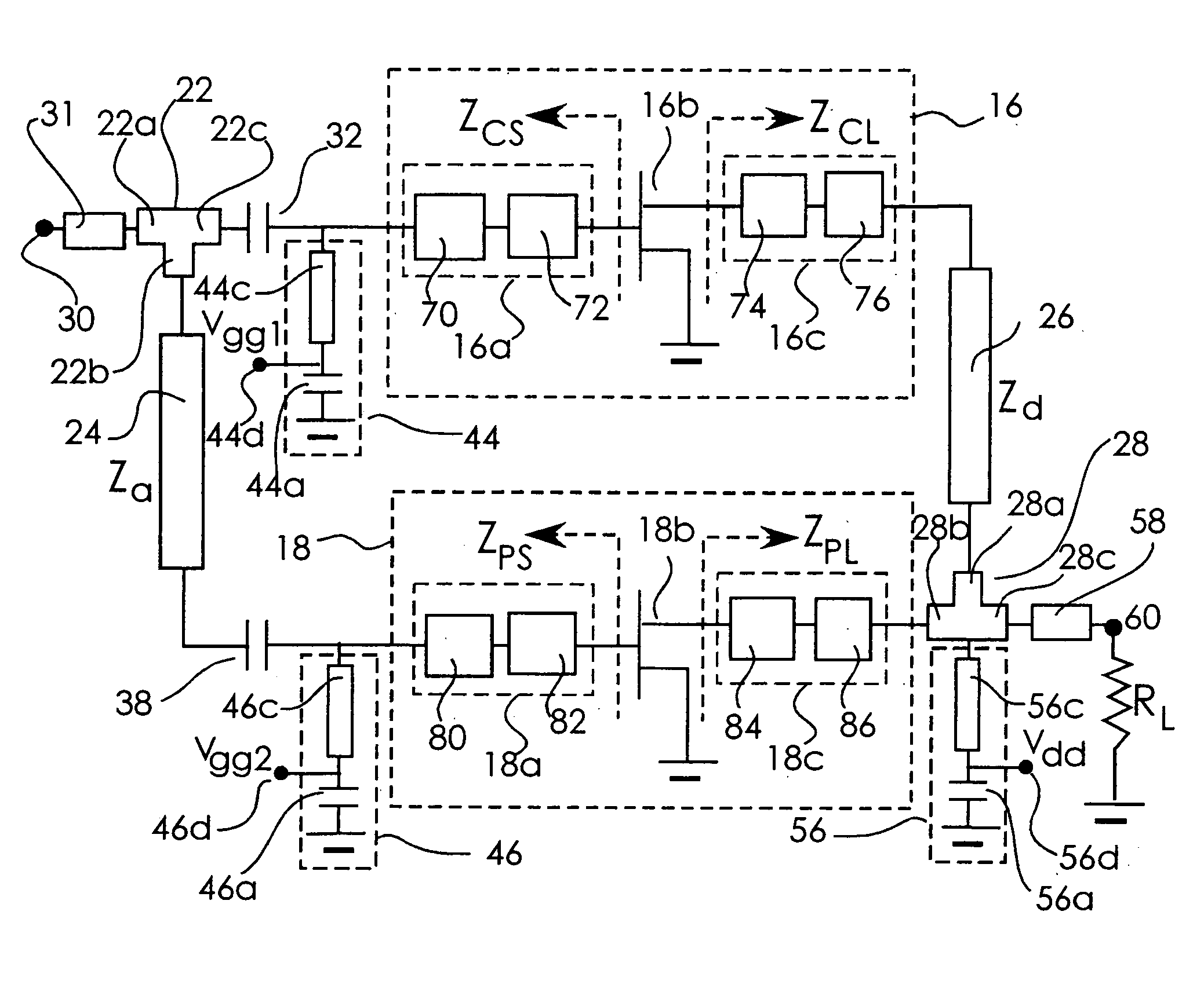
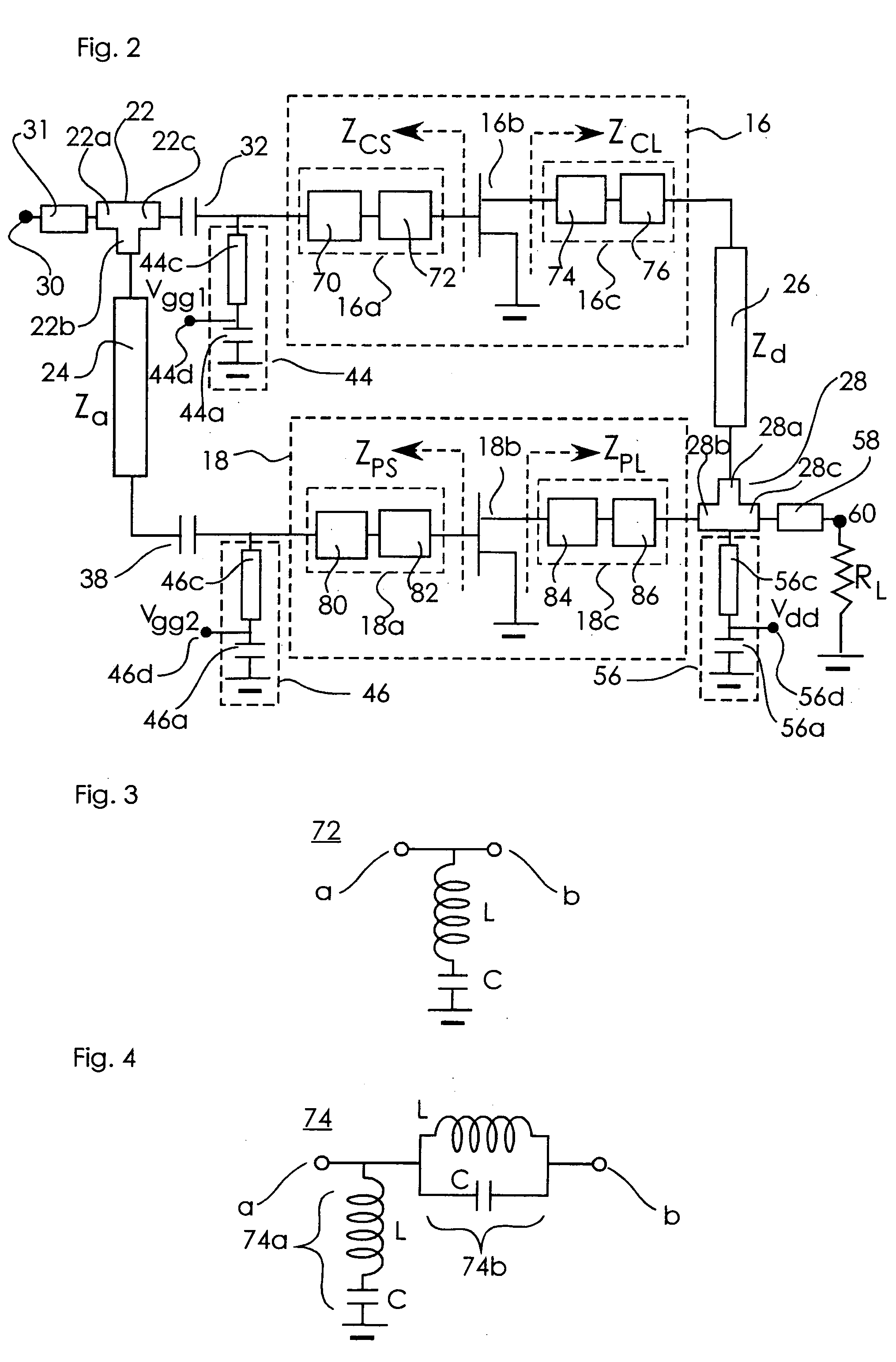
The present invention provides a high-frequency power amplifier that can achieve high efficiency at a low output level with a larger offset backoff from a maximum output. The amplifier has a unique structure that allows for a smaller package size and a smaller output higher harmonic load. The amplifier includes a divider circuit, a first amplifier circuit, a first impedance conversion circuit, a second amplifier circuit, and a combiner circuit. The first amplifier circuit performs a class F operation, while the second amplifier circuit performs a class inverse-F operation, resulting in improved efficiency in a low output level range. The amplifier can be used in microwave-band and millimeterwave-band communications equipment for mobile communication, satellite communication, and the like.

Problems solved by technology

If, however, an input signal level is sufficiently lower than a maximum output level, that is, if offset backoff (hereinafter referred to as “OBO”) is sufficiently large, then the efficiency is low accordingly.
This has been making it difficult to achieve high efficiency.
In this Doherty amplifier, however, a problem arises in that the carrier amplifier and the peak amplifier use transistors of significantly different sizes, so that its divider circuit and combiner circuit inevitably have complicated configurations.
If operating frequencies are low, then these circuits inevitably become extremely large, resulting in an increased size of the whole amplifier.
This, however, involves a complicated configuration.
Furthermore, since a plurality of the phase compensating circuits and the peak amplifiers are provided, so that the phase compensating circuits take up even more area accordingly, making it difficult to accomplish a compact amplifier.

Method used


Image

  • Power amplifier
  • Power amplifier
  • Power amplifier

Examples


first embodiment

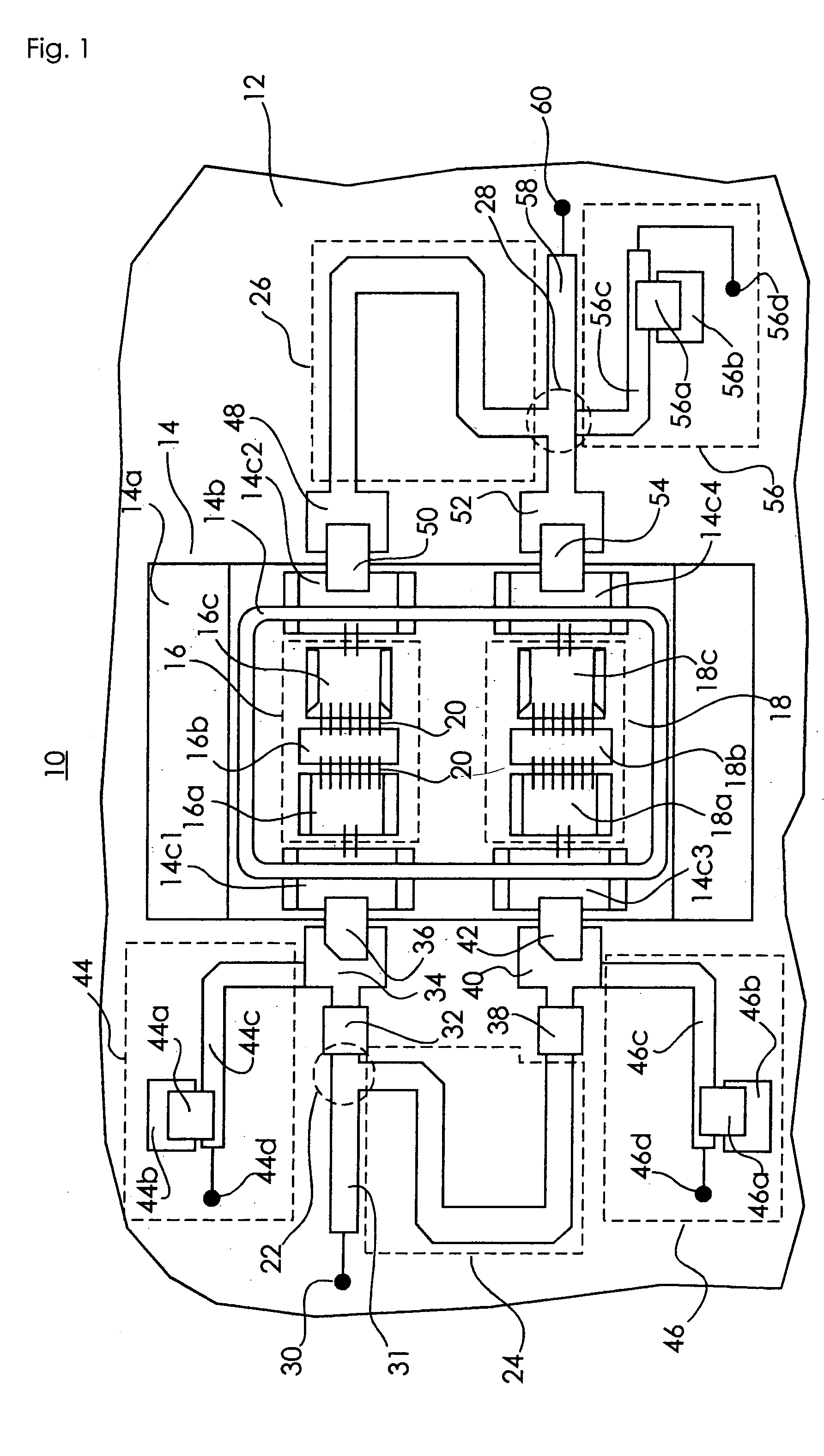
[0051]FIG. 1 is a plan view of a high-frequency power amplifier according to one embodiment of the present invention.

[0052]Referring to FIG. 1, a Doherty amplifier 10, which is an example of the first embodiment, uses a board 12 formed of, for example, a polytetrafluoroethylene member (hereinafter referred to as “PTFE”) serving as a circuit board.

[0053]As a material for the circuit board, a dielectric having a specific inductive capacity of about 2 to about 5 is used. In addition to PTFE having a specific inductive capacity of about 2.6, glass epoxy or the like having a specific inductive capacity of about 4.4 may be used.

[0054]A metal package 14 formed of a copper-molybdenum laminated material or CuW is disposed on the PTFE board 12.

[0055]The package 14 includes a metal substrate 14a, a wall 14b that is formed on the metal substrate 14a to surround a central portion of the metal substrate, and four connecting terminals 14c (14c1, 14c2, 14c3, and 14c4) for connecting internal circui...

first modification

[0104]FIG. 12 is a circuit diagram showing a modification of the high-frequency power amplifier according to an embodiment of the present invention.

[0105]In a Doherty amplifier 88 shown in FIG. 12, the second branch of the divider circuit 22 is further split into two branches and the first branch of the combiner circuit is further split into two branches so as to connect another phase compensating circuit 24 and another peak amplifier 18 between the second branch of the divider circuit 22 and the first branch of the combiner circuit in parallel to a phase compensating circuit 24 and a peak amplifier 18 disposed between the second branch of the divider circuit 22 and the second branch of the combiner circuit in the Doherty amplifier 10 shown in FIGS. 1 and 2.

[0106]Thus, using a plurality of peak amplifiers 18 provides the same effect as that obtained by increasing the size of the second FET chip 18b of the peak amplifier 18, making it possible to improve the efficiency of the amplifi...

second embodiment

[0109]FIG. 13 is a plan view of a high-frequency power amplifier according to another embodiment of the present invention. FIG. 14 is a circuit diagram of a high-frequency power amplifier according to the embodiment of the present invention.

[0110]FIGS. 13 and 14 show a Doherty amplifier 90, which is an example of the second embodiment.

[0111]The Doherty amplifier 90 shares the same basic construction as the Doherty amplifier 10 according to the first embodiment. The Doherty amplifier 90 differs from the Doherty amplifier 10 in that the Doherty network 26, which is disposed on the PTFE board 12 in the Doherty amplifier 10, has been replaced by a smaller Doherty network 92, which includes a dielectric board 92a formed of a dielectric having a higher specific inductive capacity than that of the PTFE board 12. The dielectric board 92a uses, for example, barium titanate (BaTiO3) having a specific inductive capacity of approximately 38. A microstrip line 92b having an electrical length equ...


PUM


Abstract

In a power amplifier a Doherty amplifier is provided with an output higher harmonic reflection circuit that is connected to the output terminal of a first FET chip and sets an even-numbered higher harmonic load of an output signal at the output terminal to be a short-circuit, or at a low impedance approximating a short-circuit, and sets an odd-numbered higher harmonic load of an output signal at the output terminal to be an open-circuit, or a high impedance approximating an open-circuit.

Description

BACKGROUND OF THE INVENTION[0001]1. Field of the Invention[0002]The present invention relates to a high-frequency power amplifier and, more particularly to improvement of a Doherty high-frequency power amplifier used with microwave-band and millimeterwave-band communications equipment for mobile communication, satellite communication or the like.[0003]2. Description of the Related Art[0004]In recent years, there has been an increasing demand for smaller, higher-output communications equipment used in a microwave band and a millimeter wave band. In addition, there has been also an increasing demand for higher quality of propagated signals. With this trend, needs for high-frequency power amplifiers with less distortion have been increasing.[0005]Especially a microwave communications system using multi-carrier signals or recent modulated-wave signals based on the CDMA method or the like actuates an amplifier at an output level that is far lower than its maximum power rating in order to...

Claims


Application Information

Patent Timeline
Patent Type & Authority Patents(United States)
IPC IPC(8): H03F3/68H03F1/02H03F1/07H03F3/193H03F3/60H05K1/05H05K1/14
CPCH03F1/0288H03F3/60H03F3/604H05K1/141H05K1/05
Inventor GOTOU, SEIKIINOUE, AKIRA
Owner MURATA MFG CO LTD
Learn More