Polishing apparatus and substrate processing apparatus

a technology of processing apparatus and substrate, which is applied in the direction of grinding machine components, manufacturing tools, lapping machines, etc., can solve the problems of low k film strength, high cost, and high cost, and achieve the effect of preventing the waste of polishing

Active Publication Date: 2010-03-23
EBARA CORP
View PDF28 Cites 37 Cited by
  • Summary
  • Abstract
  • Description
  • Claims
  • Application Information

AI Technical Summary

Benefits of technology

[0006]The present invention has been made in view of the above drawbacks. It is an object of the present invention to provide a polishing apparatus capable of preventing the polishing wastes and the particles produced in the polishing process from attaching to the surface of the substrate during the polishing process and the subsequent processes such as the transferring of the substrate, and to provide a substrate processing apparatus having such a polishing apparatus.
[0008]According to the present invention, since the liquid is supplied to the front and rear surfaces of the substrate during the polishing, the polishing wastes and particles are prevented from attaching to the device part of the substrate. Further, since the internal pressure of the polishing chamber can be lower than the external pressure of the polishing chamber by the evacuation of the polishing chamber through the gas outlet passage, it is possible to prevent the polishing wastes from being scattered around the polishing chamber and thus to prevent the polishing wastes from entering a region where a high cleanliness is required. Furthermore, since the polishing tape supply mechanism is disposed outside the polishing chamber, the polishing chamber can be small and can easily be kept clean.
[0012]According to the present invention, it is possible to polish not only the bevel portion but also the edge portion of the substrate. Therefore, the polishing rate (removal rate) can be improved.
[0014]According to this structure, the portion, which is being polished, of the substrate can be cooled and the removal of the polishing wastes can be accelerated. Further, it is possible to prevent the polishing wastes from attaching to the front and rear surfaces of the substrate.
[0019]With this structure, the polishing wastes can be prevented from attaching to the polishing tape, and the polishing process can be accelerated.
[0021]With this structure, the polishing wastes and particles attached to an inner surface of the housing, the rotational table, the polishing head, and other equipment can be washed out by the pure water, and hence the polishing chamber can be kept clean.

Problems solved by technology

One of the major problems in managing particles is dust caused by surface roughness produced at a bevel portion and an edge portion of a semiconductor wafer (substrate) in a fabrication process of semiconductor devices.
If Cu formed on the peripheral portion of the semiconductor wafer is attached to an arm of a transfer robot or a cassette in which the semiconductor wafer is accommodated, Cu may be diffused to contaminate other processes, resulting in a so-called cross contamination.
Since low-k film has a very low strength, it may be detached from the peripheral portion of the semiconductor wafer during CMP process and may damage, e.g. scratch, a patterned surface.
However, when the polishing tape is in sliding contact with the peripheral portion of the substrate, polishing wastes (shavings) are scattered around the substrate.
If such polishing wastes are attached to the device part of the substrate, defects may be caused in this device part, resulting in a low yield.

Method used


Image

  • Polishing apparatus and substrate processing apparatus
  • Polishing apparatus and substrate processing apparatus
  • Polishing apparatus and substrate processing apparatus

Examples


Embodiment Construction

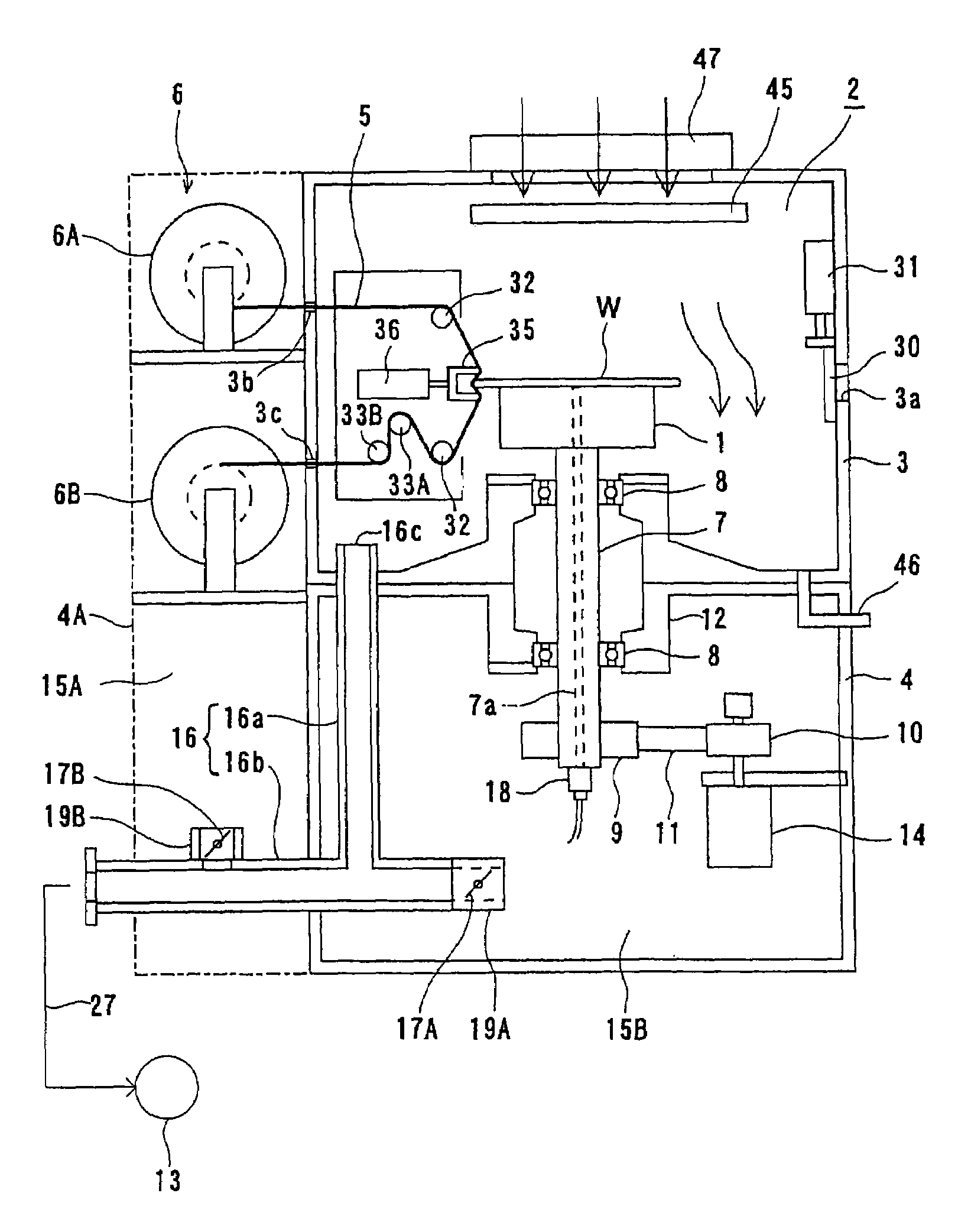
[0043]A polishing apparatus according to an embodiment of the present invention will be described below with reference to the drawings. The polishing apparatus of the present invention is designed for the purpose of polishing a bevel portion and an edge portion, i.e., a peripheral portion, of a substrate such as a semiconductor for removing surface roughness and unwanted films formed on the peripheral portion of the substrate.

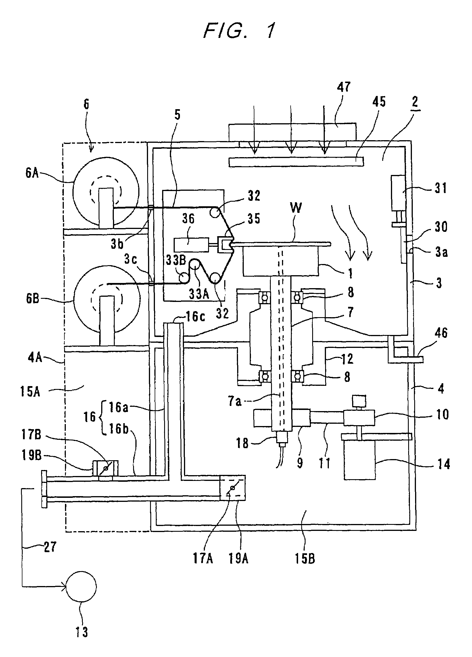
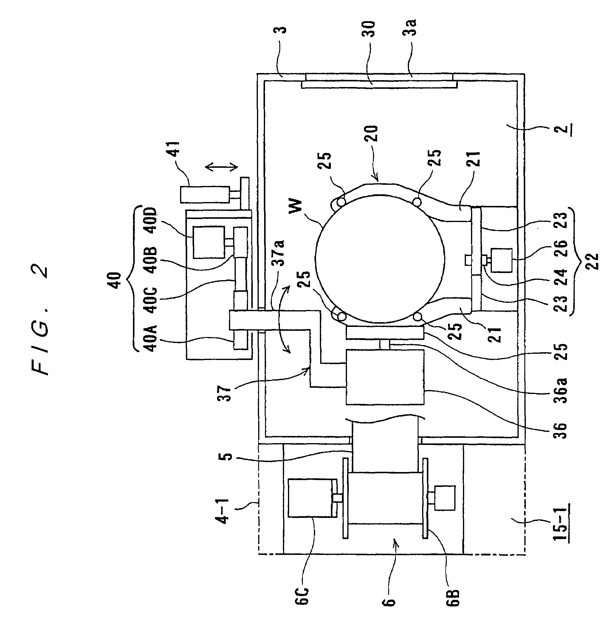
[0044]FIG. 1 is a vertical cross-sectional view showing the polishing apparatus according to the embodiment of the present invention, and FIG. 2 is a transverse cross-sectional view of the polishing apparatus shown in FIG. 1.

[0045]As shown in FIGS. 1 and 2, the polishing apparatus comprises a rotational table 1 for holding and rotating a semiconductor wafer W, an upper housing 3 having a polishing chamber 2 formed therein, a lower housing 4 disposed below the upper housing 3, a side housing 4A provided next to the upper housing 3 and the lower housing 4, and a ...


PUM


Abstract

The present invention relates to a polishing apparatus for removing surface roughness produced at a peripheral portion of a substrate, or for removing a film formed on a peripheral portion of a substrate. The polishing apparatus includes a housing for forming a polishing chamber therein, a rotational table for holding and rotating a substrate, a polishing tape supply mechanism for supplying a polishing tape into the polishing chamber and taking up the polishing tape which has been supplied to the polishing chamber, a polishing head for pressing the polishing tape against a bevel portion of the substrate, a liquid supply for supplying a liquid to a front surface and a rear surface of the substrate, and a regulation mechanism for making an internal pressure of the polishing chamber being set to be lower than an external pressure of the polishing chamber.

Description

BACKGROUND OF THE INVENTIONI. Technical Field[0001]The present invention relates to a polishing apparatus and a substrate processing apparatus, and more particularly to a polishing apparatus for removing surface roughness produced at a peripheral portion (a bevel portion and an edge portion) of a substrate such as a semiconductor wafer, or for removing a film formed on a peripheral portion of a substrate, and to a substrate processing apparatus having such a polishing apparatus.II. Description of the Related Art[0002]In recent years, according to finer structures and higher integration of semiconductor devices, it has become more important to manage particles. One of the major problems in managing particles is dust caused by surface roughness produced at a bevel portion and an edge portion of a semiconductor wafer (substrate) in a fabrication process of semiconductor devices. In this case, a bevel portion means, as shown in FIG. 11, a portion B having a curvature in a cross-section ...

Claims


Application Information

Patent Timeline
Patent Type & Authority Patents(United States)
IPC IPC(8): B24B21/00B24B9/00B24B9/06B24B37/02B24B37/04H01L21/304
CPCB24B9/065B24B37/02B24B21/002H01L21/304
Inventor HONGO, AKIHISAITO, KENYAYAMAGUCHI, KENJINAKANISHI, MASAYUKI
Owner EBARA CORP
Why Eureka
Try Eureka