Light-emitting diode arrays and methods of manufacture

a technology of light-emitting diodes and arrays, which is applied in the direction of spectral modifiers, solid-state devices, lighting and heating apparatus, etc., can solve the problems of front-of-screen performance and lcd displays are still inferior to conventional crt displays

Active Publication Date: 2010-03-30
INNOLUX CORP
View PDF3 Cites 89 Cited by
  • Summary
  • Abstract
  • Description
  • Claims
  • Application Information

AI Technical Summary

Problems solved by technology

The front-of-screen performance (contrast, brightness, viewing angle, switching times, uniformity, color gamut) of LCD displays is nevertheless still inferior to that of conventional CRT displays.

Method used


Image

  • Light-emitting diode arrays and methods of manufacture
  • Light-emitting diode arrays and methods of manufacture
  • Light-emitting diode arrays and methods of manufacture

Examples


first embodiment

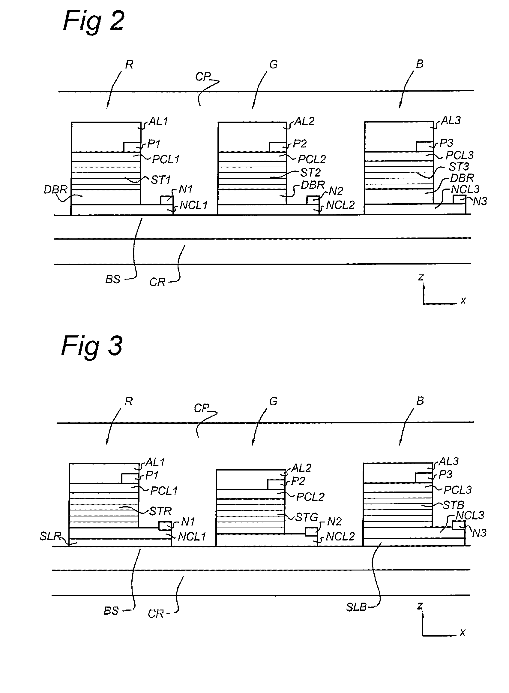
[0041]FIG. 2 shows schematically a cross-section of an LED stack arrangement. The cross-section extends along the horizontal direction X.

[0042]A base substrate BS is arranged on a carrier plate CR. The carrier plate CR has the function of being a carrier of the LED array(s) and usually may not have a required surface condition which allows forming a suitable semiconductor stack for each type R, G, B of LED element.

[0043]Thus, on top of the carrier plate CR the base substrate is arranged as an interfacial layer for each type of LED element in such a way that the interfacial layer provides substantially the required or acceptable surface condition for a type of LED element. The carrier plate CR may therefore require a treatment in order to be able to carry a base (monocrystalline) substrate BS like silicon (Si), sapphire, silicon-carbide (SiC) or gallium-arsenide (GaAs), depending on the particular semiconductor stack desired for a specific sub-pixel.

[0044]In this embodiment, the base...

second embodiment

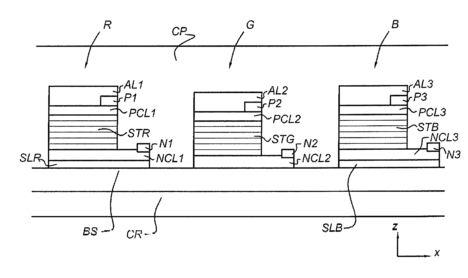
[0057]FIG. 3 shows schematically a cross-section of a LED stack arrangement. In FIG. 3, entities with the same reference number as in the preceding figures refer to the corresponding entities.

[0058]In this embodiment, different LED elements (that is, LEDs with different semiconductor stacks) are formed on the base substrate by providing a precursor layer or adhesion layer between the base substrate and the respective semiconductor stack. In the example shown here, the base substrate BS is arranged for accommodating one type of LED element directly on the surface BS by providing a specific or acceptable structural correlation with the crystal lattice of the semiconductor stack. For example, the LED element for the green sub-pixel G is grown / formed directly on the base substrate BS. The base substrate BS may provide the specific or acceptable surface condition that allows formation of the LED element with semiconductor stack STG for the green sub-pixel G directly on the base substrate...

third embodiment

[0062]FIG. 4 shows schematically a cross-section of an LED stack arrangement. In FIG. 4, entities with the same reference numbers as in the preceding figures refer to the corresponding entities.

[0063]In this example the LED element for the green sub-pixel G and the LED element for the blue sub-pixel B are formed directly on the base substrate BS. For example, the base substrate BS is specific for the negative contact layer NCL2 and the semiconductor stack ST2 of the green sub-pixel LED element G. The LED element for the green sub-pixel has, for example, an optimal structural correlation with the base substrate BS. The semiconductor stack ST3 of the blue-pixel has a less than optimal match to the base substrate BS, but the light output of the blue-pixel LED element may still be acceptable.

[0064]In this embodiment, the LED element for the red sub-pixel cannot be formed on the base substrate due to an unacceptable mismatch to the base substrate. Therefore, a precursor / adhesion layer SL...


PUM


Abstract

A representative LED array includes: a base substrate (BS) and a plurality of light emitting diodes, each of the light emitting diodes comprising a stack of a first contact layer, a semiconductor stack and a second contact layer, the semiconductor stack being on top of the first contact layer, the second contact layer being on top of the semiconductor stack; the plurality of light emitting diodes being arranged in pixel matrix on the base substrate as LEDs of at least three types (R, G, B); the LEDs according to their type (R, G, B) being arranged as at least a first, second and third sub-pixel in the pixel matrix for emission of radiation of a respective specific at least first, second and third color; and interconnection circuitry on the substrate, operative to connect to the light emitting diodes of the array for addressing each of the light emitting diodes.

Description

TECHNICAL FIELD[0001]The present invention relates to light-emitting diode (LED) arrays and methods for manufacturing such arrays.DESCRIPTION OF THE RELATED ART[0002]Nowadays, many display types exist, from conventional CRT (cathode ray tube) displays used for television and monitor applications to AM (active matrix) LCD (liquid crystal display) displays for television, monitor and mobile phone applications. The AM LCD's are emerging rapidly due to their form factor. Thin film transistor (TFT) technology enables a pixel array plate that allows for flat panel systems. The front-of-screen performance (contrast, brightness, viewing angle, switching times, uniformity, color gamut) of LCD displays is nevertheless still inferior to that of conventional CRT displays. The main reason is that the CRT is an emissive display type whereas the LCD is transmissive, reflective or both (transflective).[0003]Flat panel array plates can also used in AM OLED (organic light emitting diode) displays tha...

Claims


Application Information

Patent Timeline
Patent Type & Authority Patents(United States)
IPC IPC(8): H01L33/00F21V9/40
CPCH01L27/156
Inventor LOUWSMA, HENDRIK KLAASGOLDHOORN, PIETERJANS, HERMANS
Owner INNOLUX CORP
Why Eureka
Try Eureka