LED display utilizing freestanding epitaxial LEDs

a freestanding, led display technology, applied in the field of display apparatuses, can solve the problems of display performance issues such as jitter, color gamut, stability, etc., and achieve the effects of enhancing orientation and/or performance, preventing shorting issues, and low cos

Inactive Publication Date: 2010-03-11
GOLDENEYE
View PDF8 Cites 154 Cited by
  • Summary
  • Abstract
  • Description
  • Claims
  • Application Information

AI Technical Summary

Benefits of technology

[0020]While visible emission is possible with the FLEDs, the preferred embodiment for this invention is UV emitting FLEDs with a peak emission wavelength less than 450 nm. In one embodiment of this invention, wavelength conversion materials are used to create the visible emission required. This eliminates the need for increased drive complexity as required when multiple emission wavelength LEDs are used. It also allows for the addition of other colors via additional luminescent materials.
[0033]This invention creates microdisplays where multiple pixels are formed in the freestanding GaN epichip with interconnects and optical elements on each LED such that a line or microdisplay may be formed. The unique nature of the substrate less LED enables these novel LED arrays and displays to be formed inexpensively and with high efficiency.

Problems solved by technology

The light source constitutes a significant cost of the display.
The main cost in these types of displays remains the LCD panel itself.
Due to the complexity of the LCD panel, multi-billion dollar manufacturing facilities are required to fabricate these large area LCD panels.
Even with such a formidable infrastructure, display performance issues such as jitter, color gamut, and stability still exist.
In addition, the life and durability of these displays are handicapped by the multiple elements required to form the display.
For example the backlight has a limited life.
Emissive display approaches such as plasma (PDP) and secondary emission displays (SEDs) all offer some benefits versus LCD but suffer from the need for an evacuated cavity and life issues associated with high energy electrons bombarding the luminescent materials (light emissive layer, e.g. phosphor).
These large area digital displays are quite expensive requiring hundreds of thousands of discrete LEDs and high electrical power to drive them.
Discrete LEDs are bulky requiring mounting means and interconnection means to address each LED.
This has limited their use to large LED displays.
However, this still required complex (expensive) means to connect and address the LEDs.
With the aforementioned drawbacks to LED displays, the industry has sought means to fabricate smaller arrays of LEDs with limited success.
However, this requires tedious alignment of the LEDs to printed rows and columns of electrodes, which complicates the manufacturing process.
This, combined with expensive processing steps (e.g. MOCVD) to fabricate inorganic LEDs, makes a direct view display prohibitively expensive using arrays of inorganic LEDs.
This increases the cost of manufacturing LEDs and also limits the physical size of the LED.
These factors make it difficult and expensive to form small pixel high resolution displays using miniature LEDs as the emissive pixel.
However, the inherent nature of organic materials and their interaction with each other and the environment has forced manufacturers to use exotic encapsulation techniques with its associated cost penalties.
Even using glass panels to encapsulate and protect the organic LEDs from the environment has not met with unqualified success as OLED displays have been plagued with short lifetimes. Inorganic LEDs, as contrasted with organic LEDs, have exhibited long lifetimes and are inherently environmentally stable.
This approach limits the efficiency of such a device.
However, they are typically made via semiconductor wafer processing which is difficult to scale to large formats.
Sliced, diced, and packaged inorganic LEDs have been assembled into large area displays, however, the cost and complexity of such displays have limited this type of display to very large commercial applications.

Method used


Image

  • LED display utilizing freestanding epitaxial LEDs
  • LED display utilizing freestanding epitaxial LEDs
  • LED display utilizing freestanding epitaxial LEDs

Examples


Embodiment Construction

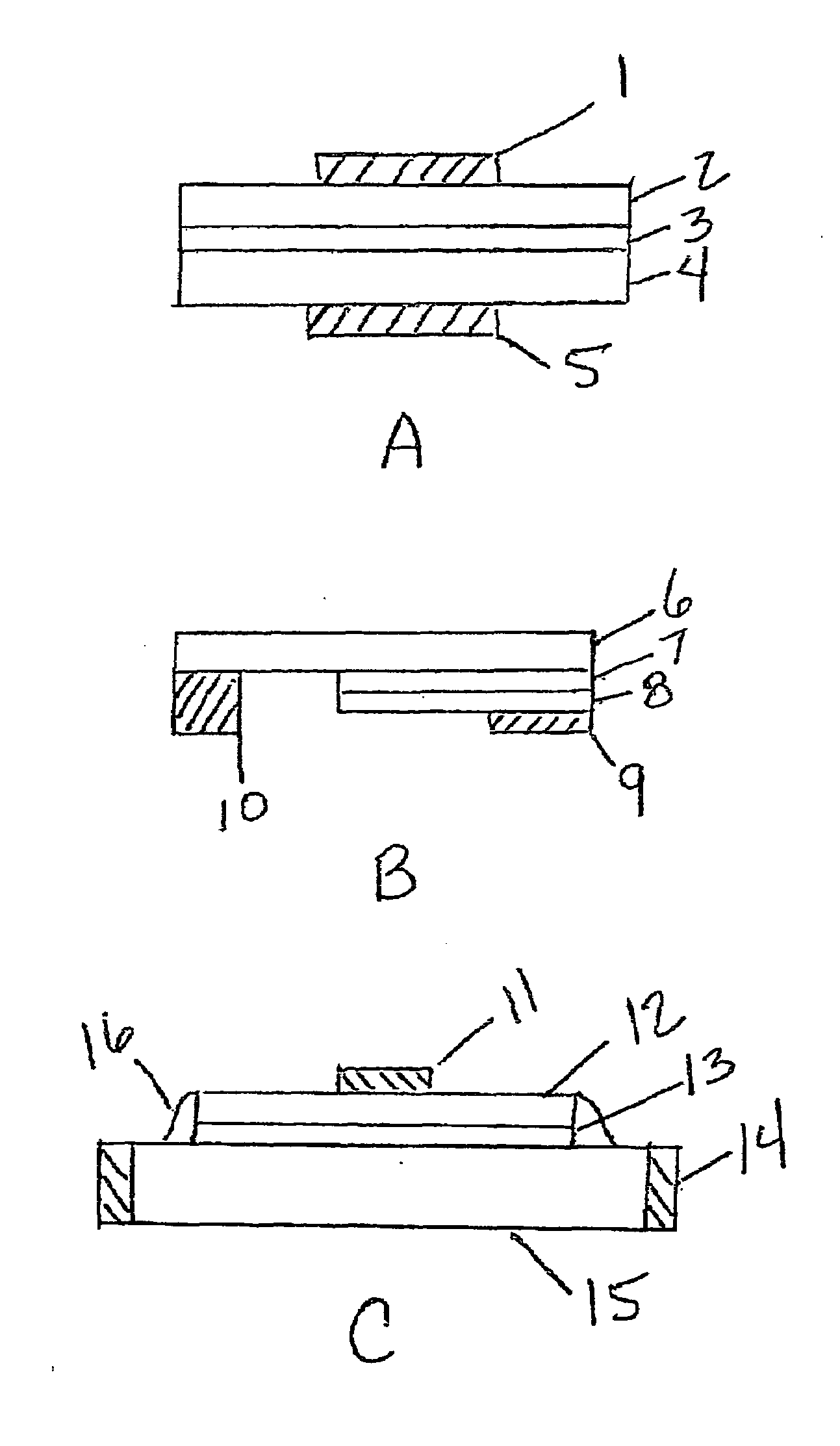
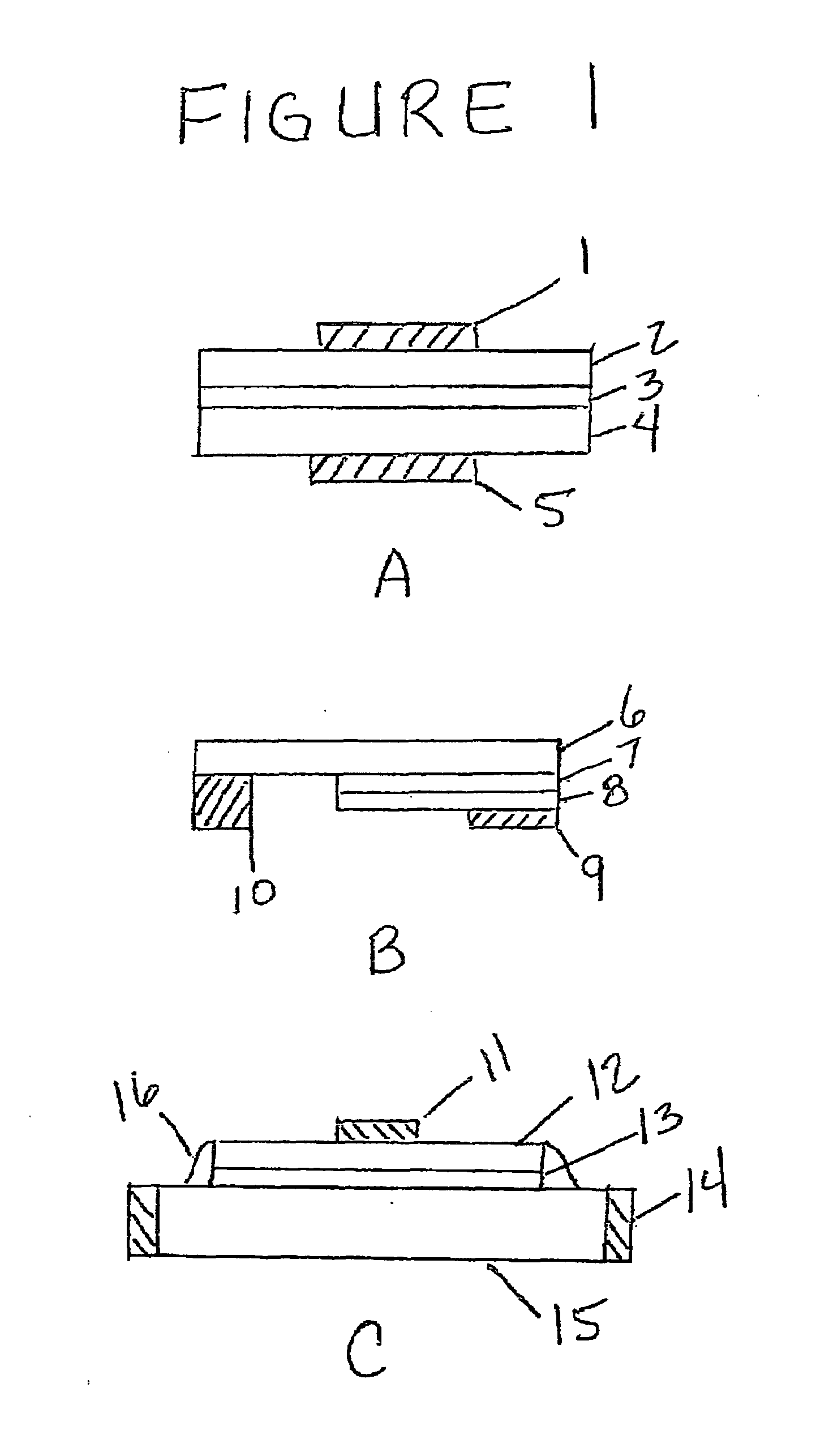
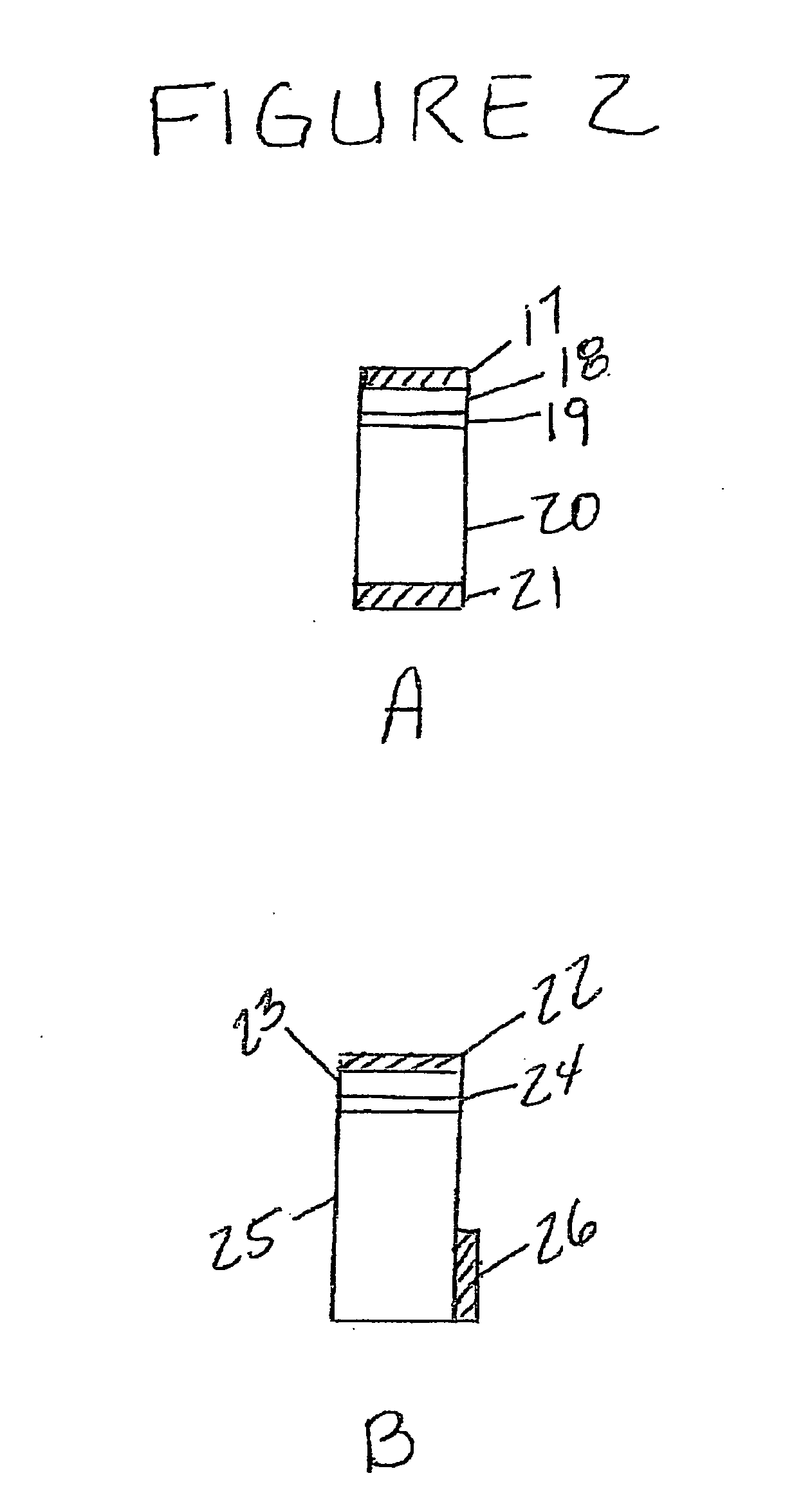
[0053]The LED addressable display is based on a freestanding epitaxial LED chip (Epichip). One method to fabricate these unique LEDs utilizes growing thick (10-100 micron) doped GaN on sapphire via HVPE, then growing PN junction & multiple quantum wells by MOCVD.

[0054]A method for fabricating mechanically robust, self-standing epitaxial layer LEDs is shown in U.S. patent application Ser. No. 12 / 148,894, commonly assigned as the present application and herein incorporated by reference. This process is modified slightly to fabricate LEDs for a printable display. A process for fabricating ultra thin epitaxial layer chips is described as follows: An epitaxial layer is first grown on a sapphire substrate to form a wafer. The epitaxial layer consists of an aluminum doped gallium nitride. The aluminum doped gallium nitride is grown in an epitaxial reactor using high vapor pressure epitaxy. A metal contact is deposited. This metal contact can be indium tin oxide, zinc oxide, carbon nanotube...


PUM


Abstract

High resolution light emitting diode (LED) displays can be formed from freestanding small epitaxial LED chips or small LED arrays. The addressing elements for the LED display can be active matrix backplane. The LED display may use isotropic and directional luminescent elements. The LED displays can be flat screen, fixed image, projection or low resolution or high resolution direct view. A macro freestanding epitaxial LED chip with multiple addressable pixels is described which forms a complete microdisplay.

Description

REFERENCE TO PRIOR APPLICATION[0001]This application claims the benefit of U.S. Provisional Patent Application Ser. No. 61 / 189,651 and U.S. Provisional Patent Application Ser. No. 61 / 189,650, which are herein incorporated by reference.FIELD OF THE INVENTION[0002]The present invention relates to display apparatuses such as a display having a plurality of light-emitting diodes (LEDs). More particularly, the invention relates to a high resolution multicolored LED flat panel display apparatus having a relatively simple structure which provides high brightness and high contrast, yet is inexpensive to manufacture.BACKGROUND OF THE INVENTION[0003]Direct-view flat panel displays typically consist of a light source and a spatial modulator LCD. The light source constitutes a significant cost of the display.[0004]The main cost in these types of displays remains the LCD panel itself. Due to the complexity of the LCD panel, multi-billion dollar manufacturing facilities are required to fabricate ...

Claims


Application Information

Patent Timeline
Patent Type & Authority Applications(United States)
IPC IPC(8): G09G3/28G09G3/34
CPCH01L25/0753H01L27/156H01L33/08H01L33/20H01L33/385H01L2924/12041H01L2924/09701H01L24/95H01L2924/00H01L2924/01322H01L2924/12036H01L2924/12044H01L2924/14
Inventor ZIMMERMAN, SCOTT M.BEESON, KARL W.LIVESAY, WILLIAM R.
Owner GOLDENEYE
Why Eureka
Try Eureka