Delay apparatus, and delay locked loop circuit and semiconductor memory apparatus using the same

a delay lock and loop circuit technology, applied in the field of semiconductor memory apparatus, can solve the problems of time delay, clock skew due to internal circuit, time delay, and defective operation not only in the delay lock loop circuit, and achieve the effect of maximizing the delay lock function

Inactive Publication Date: 2010-03-30
SK HYNIX INC
View PDF30 Cites 14 Cited by
  • Summary
  • Abstract
  • Description
  • Claims
  • Application Information

AI Technical Summary

Benefits of technology

[0025]Exemplary embodiments may provide a delay apparatus and a delay locked loop circuit, and a semiconductor memory apparatus using the same, that are capable of maximizing a delay locked function.

Problems solved by technology

When the clock that is input from the outside of the semiconductor memory apparatus is used inside the semiconductor memory apparatus, a clock skew due to an internal circuit, that is, a time delay, is generated.
When the phase difference between the two clocks, which cannot be corrected, departs from an operating range of the semiconductor memory apparatus, a defective operation occurs not only in the delay locked loop circuit but also in the semiconductor memory apparatus using the same.

Method used


Image

  • Delay apparatus, and delay locked loop circuit and semiconductor memory apparatus using the same
  • Delay apparatus, and delay locked loop circuit and semiconductor memory apparatus using the same
  • Delay apparatus, and delay locked loop circuit and semiconductor memory apparatus using the same

Examples


Embodiment Construction

[0039]Exemplary embodiments will now be described in detail with reference to the accompanying drawings.

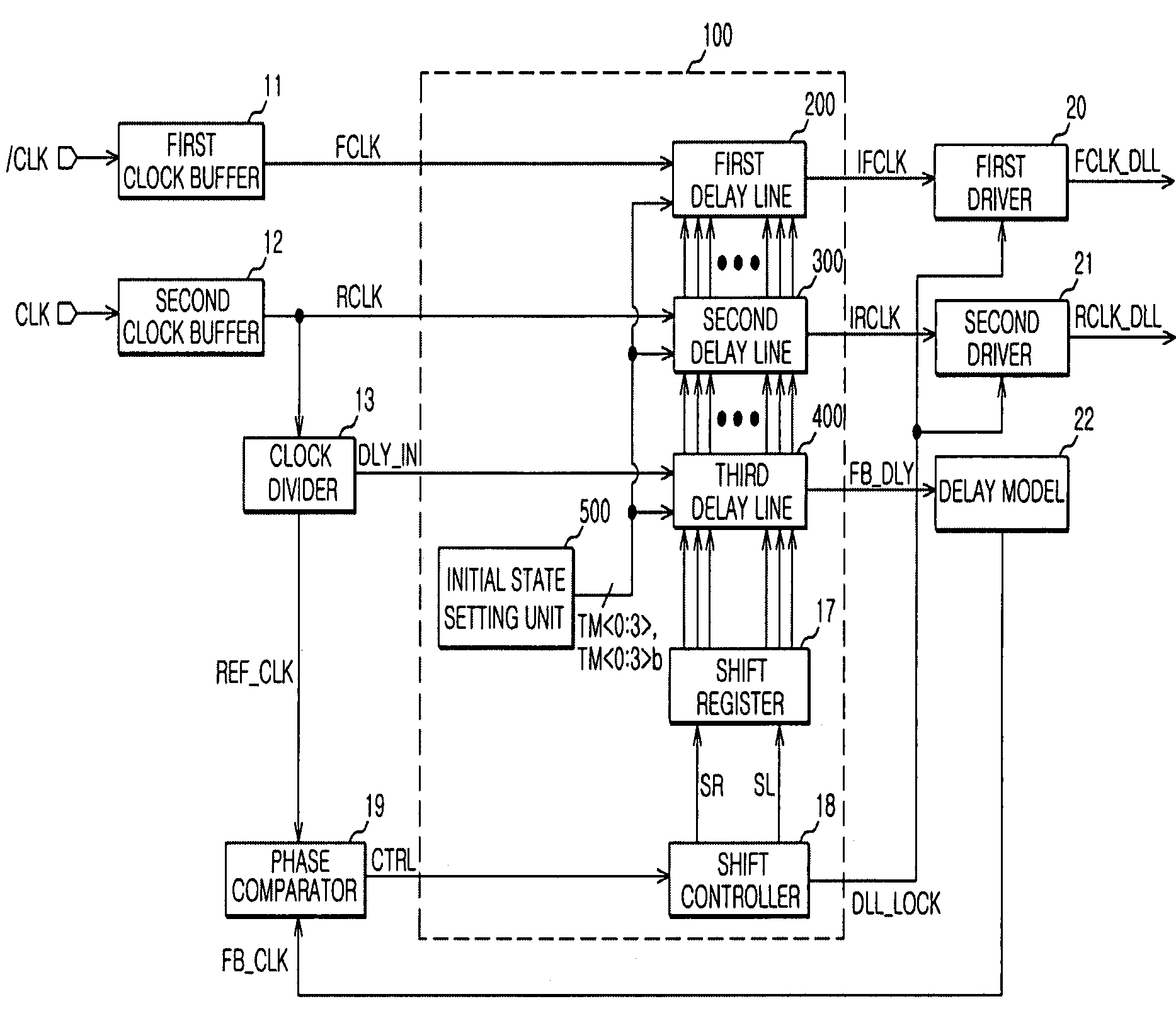
[0040]As shown in FIG. 5, a delay locked loop circuit according to one embodiment may include a first clock buffer 11, a second clock buffer 12, a clock divider 13, a register controlled delay part 100, a delay model 22, a phase comparator 19, a first driver 20, and a second driver 21. The first clock buffer 11 may receive an inverted external clock / CLK and generate a first internal clock FCLK synchronized with a falling edge of an external clock CLK. The second clock buffer 12 may receive the external clock CLK and generate a second internal clock RCLK synchronized with a rising edge of the external clock CLK. The clock divider 13 may divide the second internal clock RCLK by 1 / N, where N is a positive number, and output a delay monitoring clock DLY_IN and a reference clock REF_CLK. The register controlled delay part 100 may delay the plurality of clocks FCLK, RCLK, and DLY_IN inp...


PUM


Abstract

A delay apparatus, and a delay locked loop circuit and a semiconductor memory apparatus using the same are provided. A delay locked loop circuit includes a register controlled delay part that delays a plurality of clocks input during an initial operation by delay amounts among initial delay amounts to be varied, which are set according to initial state setting signals, and increases or decreases the set delay amounts according to a phase detecting signal after the initial operation, a phase comparator that compares a phase of any one of the plurality of clocks and a phase of any one of the plurality of clocks delayed by the register controlled delay part and outputs the phase detecting signal, and an initial state setting unit that generates the initial state setting signals.

Description

CROSS-REFERENCE TO RELATED PATENT APPLICATION[0001]This application claims the benefit of Korean Patent Application No. 10-2007-0014573, filed on Feb. 12, 2007, in the Korean Intellectual Property Office, the disclosure of which is incorporated herein in its entirety by reference.BACKGROUND OF THE INVENTION[0002]1. Technical Field[0003]Embodiments of the present invention relate to a semiconductor circuit technology, and more particularly, to a delay apparatus and a delay locked loop circuit and a semiconductor memory apparatus using the same.[0004]2. Related Art[0005]In general, clocks that are used in a semiconductor memory apparatus have been used as references to match the timing of operations, and have been used to achieve high-speed operation without the occurrence of errors. When the clock that is input from the outside of the semiconductor memory apparatus is used inside the semiconductor memory apparatus, a clock skew due to an internal circuit, that is, a time delay, is ge...

Claims


Application Information

Patent Timeline
Patent Type & Authority Patents(United States)
IPC IPC(8): H03L7/06
CPCH03H11/265H03L7/0805H03L7/0814H03L7/095G11C7/222H03K5/13
Inventor OH, YOUNG-HOON
Owner SK HYNIX INC
Why Eureka
Try Eureka