Electrophotographic photoconductor and image-forming apparatus

a photoconductor and electrotaxy technology, applied in the direction of electrotaxy, electrotaxy, instruments, etc., can solve the problems of reducing image characteristics, residual electric charges can be generated on photosensitive layers after, and the desired image characteristics cannot be constantly obtained, so as to prevent the generation of exposure memory, reduce the number of components in the apparatus, and improve the crack and wear resistance

Active Publication Date: 2010-04-20
KYOCERA DOCUMENT SOLUTIONS INC
View PDF8 Cites 5 Cited by
  • Summary
  • Abstract
  • Description
  • Claims
  • Application Information

AI Technical Summary

Benefits of technology

[0011]Therefore, as a result of intensive studies for solving the above problems, the present inventors have found that the addition of a certain hole-transfer agent and a certain additive to a photosensitive layer could prevent the generation of exposure memory for a long period in addition to improve its ability of preventing the generation of cracks due to the presence of a contaminant component.
[0012]In other words, an object of the present invention is to provide an electrophotographic photoconductor, which is excellent in crack resistance and wear resistance and also excellent in sensitivity characteristics, while keeping good image characteristics for a long period, and to provide an image-forming apparatus comprising such an electrophotographic photoconductor.

Problems solved by technology

Therefore, there is a problem in that desired image characteristics can not be constantly obtained.
However, even though the use of such a photoconductor can lead to improvements in transfer memory and repetition stability to some extent, there is another problem in that residual electric charges can be generated on a photosensitive layer after transfer.
In addition, in the process of repetitively using the photoconductor in this way, when any of contaminant components from a human body or from a contacting portion of the photoconductor has attached on the surface of the photoconductor, cracks can occur from the contaminant-attached portion, thereby causing a lowering in image characteristics.
Furthermore, these photoconductors require a process of erasing residual charges using means for neutralization of electricity as an image-forming system, so that there is a further problem in that it is difficult to cope with miniaturization of a device.

Method used


Image

  • Electrophotographic photoconductor and image-forming apparatus
  • Electrophotographic photoconductor and image-forming apparatus
  • Electrophotographic photoconductor and image-forming apparatus

Examples


first embodiment

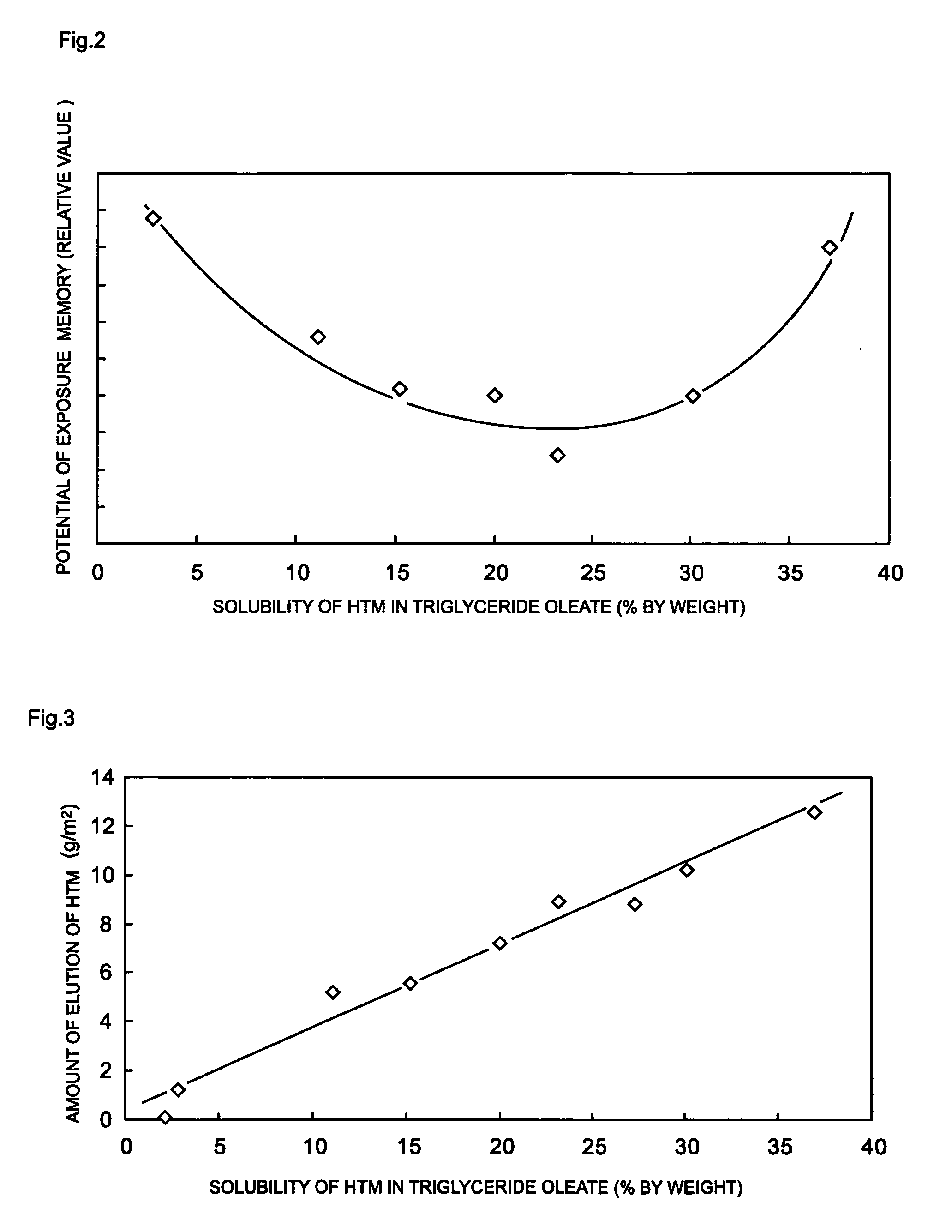
[0041]A first embodiment of the present invention is an electrophotographic photoconductor comprising a photosensitive layer containing at least a charge-generating agent, a hole-transfer agent, and a binder resin on a conductive substrate, where the hole-transfer agent has a solubility of 5 to 35% by weight with respect to triglyceride oleate and the photosensitive layer contains a compound represented by the following general formula (1) as an additive.

[0042]Hereinafter, a mono-layer type electrophotographic photoconductor as the first embodiment of the present invention will be specifically described.

1. Mono-layer Type Electrophotographic Photoconductor

(1) Basic Configuration

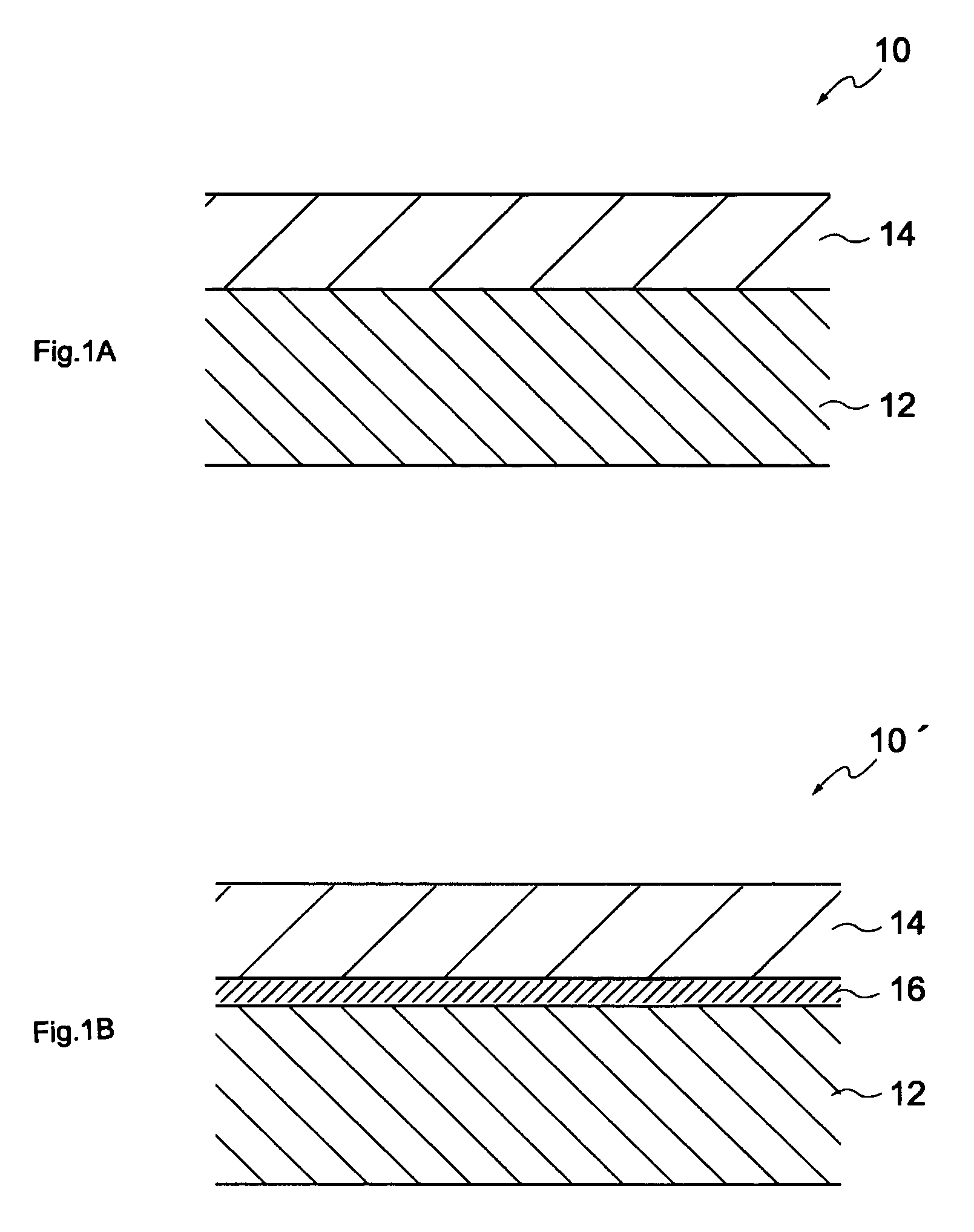
[0043]As shown in FIG. 1A, a mono-layer type electrophotographic photoconductor 10 is constructed of a single photosensitive layer 14 mounted on a conductive substrate 12.

[0044]The photosensitive layer 14 may be formed by coating the surface of the conductive substrate 12 with a coating solution and then dryi...

second embodiment

[0159]A second embodiment of the present invention is an image-forming apparatus that comprises an electrophotographic photoconductor of the first embodiment and an electrification device for carrying out an electrostatic charge process, an exposure light source for carrying out an exposure process, a developing device for carrying out an image development process, and a transfer device for carrying out an image-transferring process, which are arranged around the electrophotographic photoconductor. In addition, such an image-forming apparatus has no unit for electricity neutralization.

[0160]Furthermore, in the following description for the image-forming apparatus, it will be described with reference to an example that uses a mono-layer type photoconductor as an electrophotographic photoconductor.

[0161]As shown in FIG. 7, around an electrophotographic photoconductor 31, an electrification device 32 for carrying out an electrostatic charge process, an exposure light source 33 for carr...

example 1

1. Manufacture of Electrophotographic Photoconductor

[0167]A coating solution for preparing a photosensitive layer was prepared by dispersing and mixing 4 parts by weight of an X-type metal-free phthalocyanine (CGM-A) represented by the general formula (8) as a charge-generating agent; 50 parts by weight of a compound (HTM-1) represented by the general formula (12); 30 parts by weight of a compound (ETM-A) represented by the general formula (37) as a electron-transfer agent; 100 parts by weight of a Z-type polycarbonate resin (BD-1) (weight-average molecular weight: 35000) represented by the general formula (43) as a binder resin; and 4.5 parts by weight of a compound (BD-2) represented by the general formula (3) as an additive together with 800 parts by weight of tetrahydrofuran by means of a ball mill for 50 hours.

[0168]Next, the coating solution thus obtained was applied on two cylindrical aluminum tubes (one of 30 mm in diameter and 254 mm in length and the other of 16 mm in diam...


PUM

PropertyMeasurementUnit
Tgaaaaaaaaaa
glass transition pointaaaaaaaaaa
thicknessaaaaaaaaaa

Abstract

An electrophotographic photoconductor having an excellent crack resistance and wear resistance as well as excellent sensitivity characteristics, while keeping good image characteristics of the photoconductor is provided. In addition, an image-forming apparatus equipped with such an electrophotographic photoconductor is also provided. The electrophotographic photoconductor includes a photosensitive layer containing at least a charge-generating agent, a hole-transfer agent, and a binder resin on a conductive substrate. The hole-transfer agent has a solubility of 5 to 35% by weight with respect to triglyceride oleate and the photosensitive layer contains a compound represented by the following general formula (1) as an additive:

Description

BACKGROUND OF THE INVENTION[0001]1. Field of the Invention[0002]The present invention relates to an electrophotographic photoconductor and an image-forming apparatus provided therewith. In particular, the present invention relates to an electrophotographic photoconductor, which is excellent in contamination resistance and is capable of preventing the generation of exposure memory for a long period, and an image-forming apparatus provided with such an electrophotographic photoconductor.[0003]2. Description of Related Art[0004]Heretofore, organic photoconductors have been widely used as electrophotographic photoconductors, which contains a charge-generating agent for generating electric charges by light exposure and a charge-transfer agent for-transfer the generated charges, and a binder resin for dispersing these substances therein to form a layered structure.[0005]An image-forming apparatus using such an organic photoconductor employs an image-forming process by sequentially arrangi...

Claims


Application Information

Patent Timeline
Patent Type & Authority Patents(United States)
IPC IPC(8): G03G5/06
CPCG03G5/047G03G5/0517G03G5/0605G03G5/062G03G5/0612G03G5/0618G03G5/0609
Inventor NAKAI, NORIOHAMASAKI, KAZUNARIKUBOSHIMA, DAISUKEINAGAKI, YOSHIOOKADA, HIDEKIICHIGUCHI, TETSUYAMARUO, KEIJI
Owner KYOCERA DOCUMENT SOLUTIONS INC
Why Eureka
Try Eureka