Low read current architecture for memory

a memory array and low read current technology, applied in the direction of information storage, static storage, digital storage, etc., can solve the problems of difficult to distinguish between the read current and the leakage current, leakage current can be considered noise that masks the read current signal, and memory elements that share a row or column conductor with the memory element being read

Inactive Publication Date: 2010-04-20
UNITY SEMICON
View PDF11 Cites 73 Cited by
  • Summary
  • Abstract
  • Description
  • Claims
  • Application Information

AI Technical Summary

Problems solved by technology

One challenge that arises from a two-terminal configuration is that memory elements that share a row or column conductor with the memory element being read will also have a potential difference across their respective row and column conductors.
On the other hand, the leakage current can be considered to be noise that masks the read current signal.
A low S / N ratio can make it difficult to distinguish between the read current and the leakage current.
Consequently, the low S / N ratio makes it difficult to detect an accurate value for the stored data.

Method used


Image

  • Low read current architecture for memory
  • Low read current architecture for memory
  • Low read current architecture for memory

Examples


Embodiment Construction

[0023]In the following detailed description, numerous specific details are set forth to provide a through understanding of the present invention. It will be apparent to one skilled in the art that the present invention may be practiced without some or all of these specific details. In other instances, well known elements and process steps have not been described in depth in order to avoid unnecessarily obscuring the present invention.

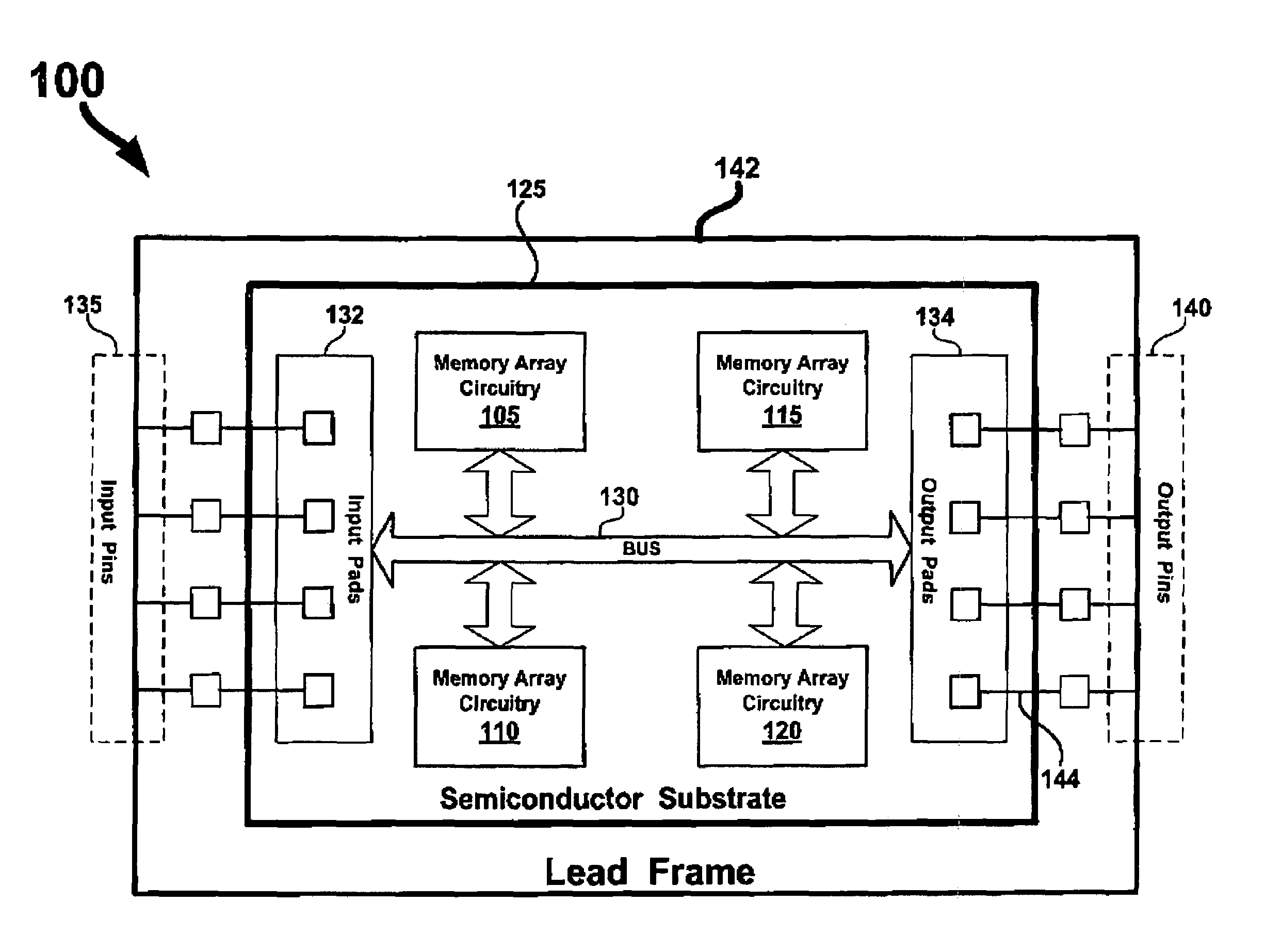
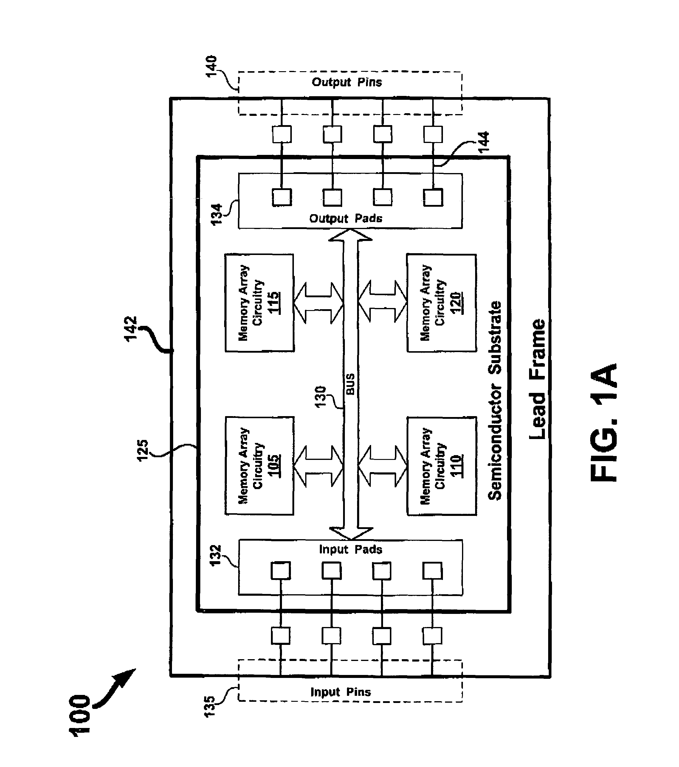
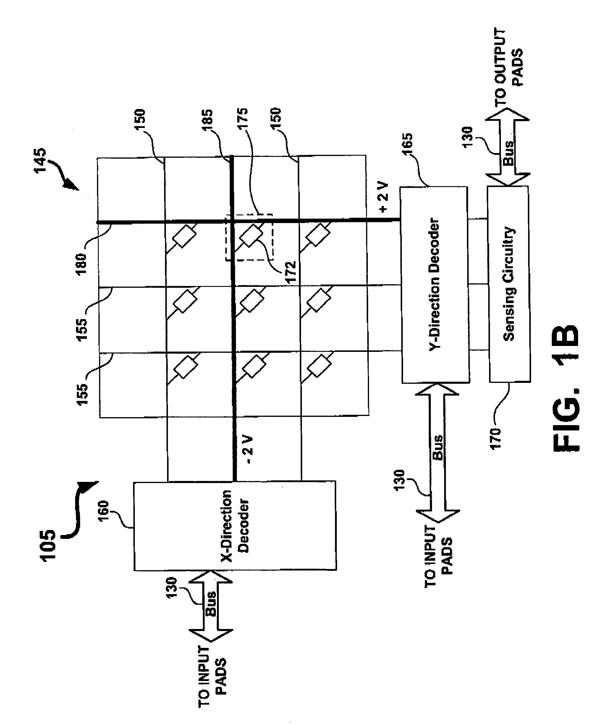
[0024]FIG. 1A is a block diagram of an integrated circuit 100 that performs memory functions. Memory array circuitry 105, 110, 115, and 120, which are typically fabricated on a semiconductor substrate 125, are components of the integrated circuit 100. Memory array circuitry 105-120 includes arrays of memory cells and associated peripheral circuitry. A bus 130 connects the memory array circuitry 105-120 to input pads 132 and output pads 134. Input pads 132 and output pads 134 are connected to input pins 135 and output pins 140 through interconnects 144, ...


PUM


Abstract

A low read current architecture for memory. Bit lines of a cross point memory array are allowed to be charged by a selected word line until a minimum voltage differential between a memory state and a reference level is assured.

Description

FIELD OF THE INVENTION[0001]The present invention relates generally to sensing a signal in a memory array. More specifically, the present invention relates to sensing a signal in a two-terminal memory array.BACKGROUND OF THE INVENTION[0002]Data storage in high-density memory devices can be accomplished using a variety of techniques. Often, the technique used depends on whether or not the stored data is volatile or non-volatile. In volatile memory devices, such as SRAM and DRAM, for example, stored data is not retained when power is removed from the memory device. On the other hand, for non-volatile memory devices, such as MRAM and Flash devices, stored data is retained when power is removed from the memory device.[0003]Resistive state memory devices are a promising new type of non-volatile memory in which data is stored in a memory element as a plurality of resistive states. A first resistive state can represent a logic “1” and a second resistive state can represent a logic “0”. The...

Claims


Application Information

Patent Timeline
Patent Type & Authority Patents(United States)
IPC IPC(8): G11C7/00
CPCG11C7/12G11C7/22G11C13/0007G11C13/0026G11C13/004G11C13/0061G11C13/02G11C2213/77G11C2013/0054G11C2213/11G11C2213/31G11C2213/32G11C2213/71
Inventor RINERSON, DARRELLCHEVALLIER, CHRISTOPHE J.SIAU, CHANG HUA
Owner UNITY SEMICON
Why Eureka
Try Eureka