Liquid crystal lens element and optical head device

a liquid crystal lens and optical head technology, applied in the field of liquid crystal lens elements and optical head devices, can solve the problems of increasing the size of the optical head device b>100/b>, writing error, writing error, etc., and achieves the effects of reducing the thickness of the liquid crystal layer, low voltage drive, and high speed respons

Inactive Publication Date: 2010-05-04
ASAHI GLASS CO LTD
View PDF15 Cites 20 Cited by
  • Summary
  • Abstract
  • Description
  • Claims
  • Application Information

AI Technical Summary

Benefits of technology

[0035]According to the present invention, since transmission wavefront changes according to the magnitude of applied voltage, it is possible to realize a focal-length-variable liquid crystal lens. Further, by the Fresnel lens surface provided in the liquid crystal lens element of the present invention, it becomes possible to reduce the thickness of liquid crystal layer, which leads to low voltage drive and high speed response. Further, by a phase correction surface provided in the liquid crystal lens element of the present invention, it is possible to provide a liquid crystal lens element having high light utilization. Accordingly, in the optical head device provided with such a liquid crystal lens element, it is possible to correct spherical aberration caused by the difference of cover thicknesses in a double-layer optical disk, and further, since the aberration scarcely deteriorates even when a misalignment occurs between an objective lens and the liquid crystal lens element at a time of tracking, an optical head device capable of stably writing and / or reading is realized.

Problems solved by technology

In particular, in a case of double-layer optical disk of writing type, deterioration of convergence corresponds to decrease of converging power density, which causes a writing error, such being a problem.
However, also in this case, with respect to a double layer optical disk of recording type, a spherical aberration generated corresponding to the difference of the cover thickness, causes a writing error, such being a problem.
However, in the case of employing the movable lens group 160, there has been a problem that the size of the optical head device 100 becomes larger since the pair of lenses 161 and 162 and the actuator 163 are required, and the mechanical design for the movement becomes complicated.
As a result, the layer of liquid crystal 270 becomes thicker, which causes problems that driving voltage increases and response becomes slower.
However, when the substrate 260 is fabricated to have a surface shape S(r) so as to correct only spherical aberration, if the optical axis of an objective lens for converging incident light on an information recording layer of an optical disk, and the optical axis of the liquid crystal lens are not aligned to each other, a coma aberration is generated which causes a problem that convergence to the information recording layer is deteriorated and writing or reading is prevented.
In this case, since no≠nF, a fixed phase difference represented by a formula φ=d×(nF−no)λ is generated for ordinarily polarized light, which has been a problem in a case of applying the liquid crystal lens to an optical head device employing a polarization optical system.
As a result, a problem that diffraction efficiency of 0-th order light decreases, is generated.

Method used


Image

  • Liquid crystal lens element and optical head device
  • Liquid crystal lens element and optical head device
  • Liquid crystal lens element and optical head device

Examples


first embodiment

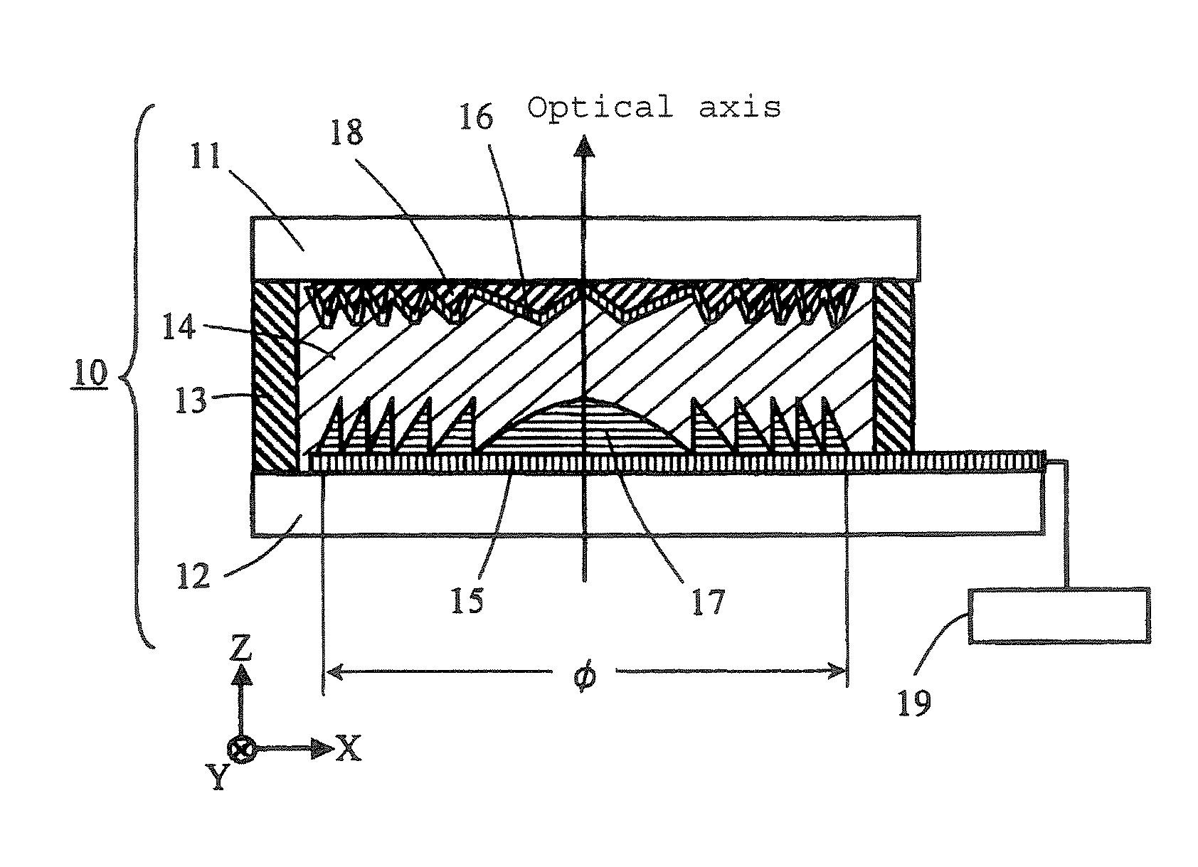
[0066]FIG. 1 is a cross-sectional view showing a first embodiment of a liquid crystal lens element of the present invention, in which a liquid crystal lens element according to this embodiment has a liquid crystal layer 14 sandwiched by transparent substrates 11 and 12 and a seal 13. On a surface of the first transparent substrate 12, a transparent electrode 15 and a Fresnel lens surface 17 are formed, and on a surface of the second transparent substrate 11, a phase correction surface 18 and a transparent electrode 16 are formed. The transparent electrodes 15 and 16 are connected with an external signal source 19 to apply a voltage to the liquid crystal layer 14. Although not shown in FIG. 1, on surfaces of the transparent electrode 16 and the Fresnel lens surface 17, alignment films for aligning the liquid crystal layer 14 are formed. Further, an antireflective film may be formed on outer surfaces of the transparent substrates 11 and 12.

[0067]Then, an example of production process ...

second embodiment

[0101]Then, an example of the construction of the liquid crystal lens element according to a second embodiment of the present invention is described as follows.

[0102]FIG. 5 is a cross-sectional view showing a liquid crystal lens element according to the second embodiment of the present invention. A liquid crystal lens element according to this embodiment has a liquid crystal layer 24 sandwiched by transparent substrates 21 and 22 and a seal 23. Among these, on a surface of the first transparent substrate 22, a transparent electrode 25 is formed. On the other hand, on a surface of the second transparent substrate 21, a phase correction surface 28, a transparent electrode 26 and a Fresnel lens surface 27 are formed in this order. The transparent electrodes 25 and 26 are connected with an external signal source 19 to apply a voltage to the liquid crystal layer 24. Here, although not shown in FIG. 5, on surfaces of the transparent electrode 25 and the Fresnel lens surface 27, alignment ...

third embodiment

[0110]Then, an optical head device employing the liquid crystal lens element of the present invention is described as follows.

[0111]FIG. 6 is a schematic view showing an example of an optical head device 30 employing the liquid crystal lens element of the present invention. The optical head device 30 is configured to write and / or read an information to / from a double layer optical disk D, and has a laser diode 31 as a light source, a polarizing beam splitter 32, a collimator lens 33, the liquid crystal lens element 10 (20) of the present invention, a quarter waveplate 35, an objective lens 36, a cylindrical lens 37 and a photodetector 38. Meanwhile, as the double layer optical disk D, e.g. a DVD or a high density optical disk is employed, which has a first recording layer D1 and a second recording layer D2.

[0112]The laser diode 31 may be a laser diode of any one of 780 nm band, 660 nm band and 405 nm band in terms of wavelength to use according to the type of optical disk D, or a plu...


PUM

PropertyMeasurementUnit
wavelength bandaaaaaaaaaa
thickaaaaaaaaaa
thicknessaaaaaaaaaa

Abstract

A liquid crystal lens element having a lens function capable of stably correcting spherical aberration containing a power component corresponding to focus change of incident light according to the magnitude of applied voltage.The liquid crystal lens element comprises a pair of transparent substrates 11 and 12, one (12) of the transparent electrodes is provided with a transparent electrode 15 and a Fresnel lens surface 17, and the other one (11) of the pair of transparent electrodes is provided with a phase correction surface 18 and a transparent electrode 16. Thus, by disposing a Fresnel lens surface 17 and a liquid crystal layer 13 between a pair of transparent electrodes 15 and 16, it becomes possible to change substantial refractive index distribution of the liquid crystal layer 13 according to the magnitude of applied voltage, and to add a positive or negative power to a wavefront transmitted through the liquid crystal layer 13, the Fresnel lens surface 17 and the phase correction surface 18.

Description

TECHNICAL FIELD[0001]The present invention relates to a liquid crystal lens element and an optical head device, in particular, to a liquid crystal lens capable of switching the focal length among different focal lengths according to a magnitude of applied voltage, and an optical head device employing the liquid crystal lens, for writing and / or reading an information to / from an optical recording medium.BACKGROUND ART[0002]As examples of an optical recording medium (hereinafter referred to as “optical disk”) having an information recording layer formed on a surface of light-incident side, and a transparent resin covering the information recording layer, e.g. CDs and DVDs are widely used. Further, in an optical head device for writing and / or reading an information to / from DVDs, one employing a laser diode of 660 nm wavelength band as a light source and an objective lens having a NA (numerical aperture) of from 0.6 to 0.65, are known.[0003]Heretofore, a commonly used DVD (hereinafter re...

Claims


Application Information

Patent Timeline
Patent Type & Authority Patents(United States)
IPC IPC(8): G02F1/13
CPCG02F1/133526G02F1/29G11B7/13925G11B7/1369G11B7/1378G02F2001/294G02F1/294G02F1/13
Inventor NOMURA, TAKUJIKOJIMA, HIROYUKI
Owner ASAHI GLASS CO LTD
Why Eureka
Try Eureka