Semiconductor device and manufacturing method thereof

a technology of semiconductors and semiconductors, applied in the field of semiconductor devices, can solve the problems of difficult transposing of memory elements, destroying elements, and not peeling properly, and achieve the effects of high adhesion, good state, and high reliability

Inactive Publication Date: 2010-05-11
SEMICON ENERGY LAB CO LTD
View PDF31 Cites 14 Cited by
  • Summary
  • Abstract
  • Description
  • Claims
  • Application Information

AI Technical Summary

Benefits of technology

[0009]In view of the foregoing problem, the present invention provides a technique capable of manufacturing a semiconductor device having a memory element having good adhesion inside the memory element, so that a transposition step can be performed with a good state maintaining the form and properties before peeling. Therefore, it is also an object of the invention to provide a technique capable of manufacturing a semiconductor device having higher reliability with a high yield without complexing the apparatus or process.
[0012]As SP values of substances get closer to each other, adhesion between the substances is increased. In general, the SP value of an organic compound material is smaller as compared to that of a metal material. Therefore, for improving the adhesion between the organic compound layer and the conductive layer, an organic compound material having an SP value as large as possible is preferably selected for the organic compound layer whereas a metal material having an SP value as small as possible is preferably selected for the conductive layer, so that difference between the SP value of the material used for the organic compound layer and the SP value of the material used for the conductive layer can be reduced.
[0015]In addition, interface tension at an interface between layers within an element also affects adhesion between the layers. As the interface tension between layers gets smaller, adhesion between the layers is increased so that a defect such as film peeling becomes harder to occur in the peeling process. Therefore, a peeling and transposing process of an element can be performed with a good form. Interface tension can be guessed from the surface tension against air, nitrogen, helium, or the like, and the surface tension of a metal is larger than that of an organic material. Further, wettability of a metal material against an organic material is improved by oxidizing a surface of the metal material. Therefore, by performing oxidation treatment to an interface between the conductive layer using a metal material and the organic compound layer using an organic compound material, the interface tension can be reduced. It is preferable that the interface tension is 1.5N / m or less.
[0017]In addition, a combination of materials such that an atom of an organic material constituting the organic compound layer and an atom of a metal material constituting the conductive layer bond chemically to each other may be preferably used, thereby improving adhesion between the organic compound layer and the conductive layer.
[0029]By the present invention, a semiconductor device including a memory element which has high adhesion inside the memory element so as to perform a transposition step with a good state can be manufactured. Therefore, a semiconductor device having higher reliability can be manufactured with a high yield without complexing the apparatus or process.

Problems solved by technology

However, if adhesion between thin films for constituting the element which is to be transposed is low, there is a problem of being peeled off not properly and destroying the element.
As described above, inferior adhesion among the first conductive layer, the organic compound layer, and the second conductive layer may destroy the memory element by causing film peeling at an interface in the peeling process; therefore, it is difficult to transpose the memory element with a good state maintaining the form and properties before the peeling.

Method used


Image

  • Semiconductor device and manufacturing method thereof
  • Semiconductor device and manufacturing method thereof
  • Semiconductor device and manufacturing method thereof

Examples


embodiment mode 1

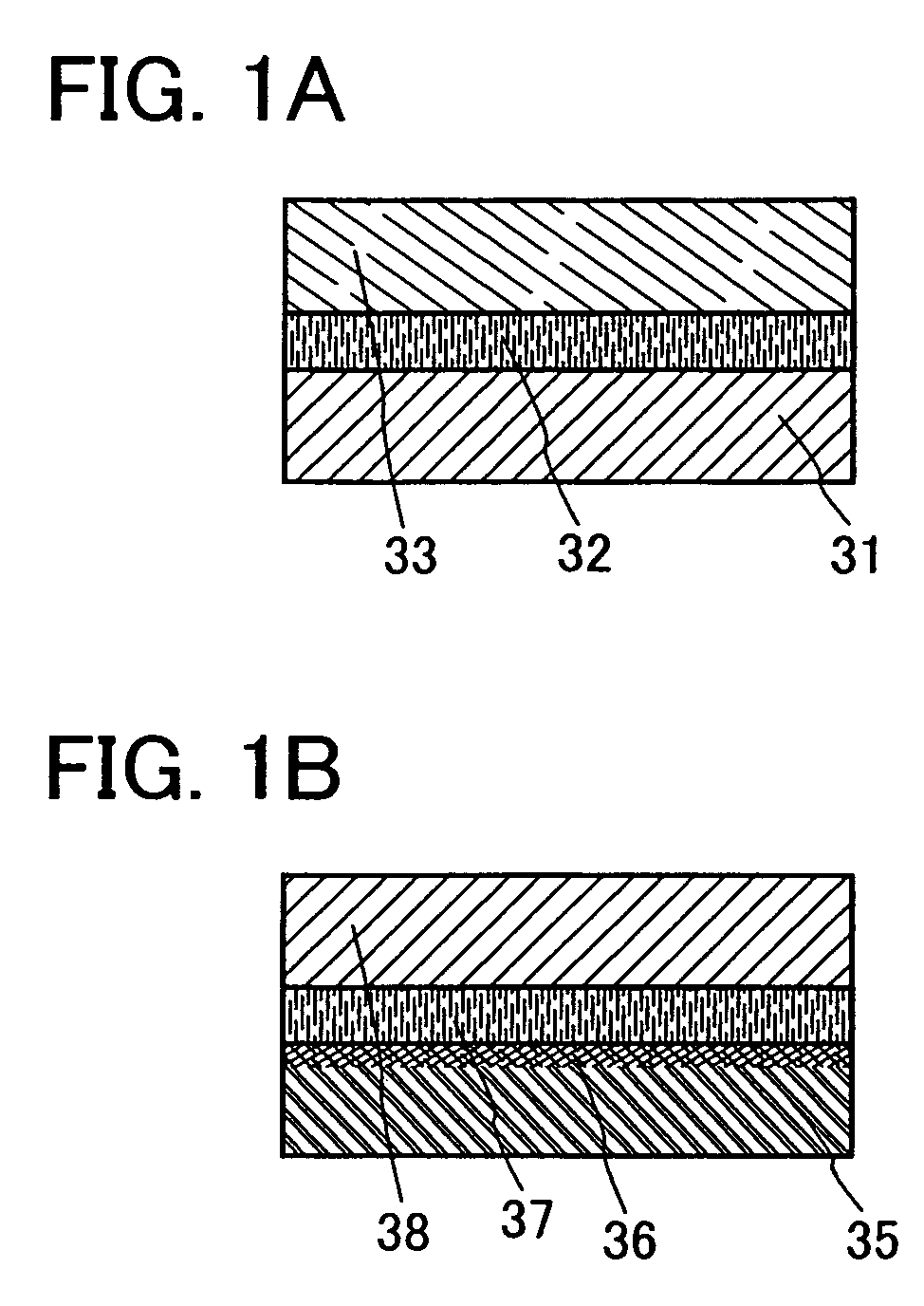
[0053]A memory element to which the present invention is applied will be described in this embodiment mode, using FIGS. 1A and 1B.

[0054]The invention focuses on adhesion between the organic compound layer and the first conductive layer and between the organic compound layer and the second conductive layer. Adhesion between substances is affected by the solubility parameter (SP value). Solubility parameter is a value of the ½-th power of the cohesive energy density (CED) of one molecule per unit volume.

[0055]As respective SP values of substances get closer to each other, adhesion between the substances is increased. In general, the SP value of an organic compound material is small as compared to that of a metal material. Therefore, for improving the adhesion between the organic compound layer and each conductive layer, an organic compound material having an SP value as large as possible may be selected for the organic compound layer whereas a metal material having an SP value as smal...

embodiment mode 2

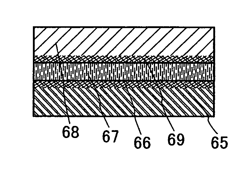
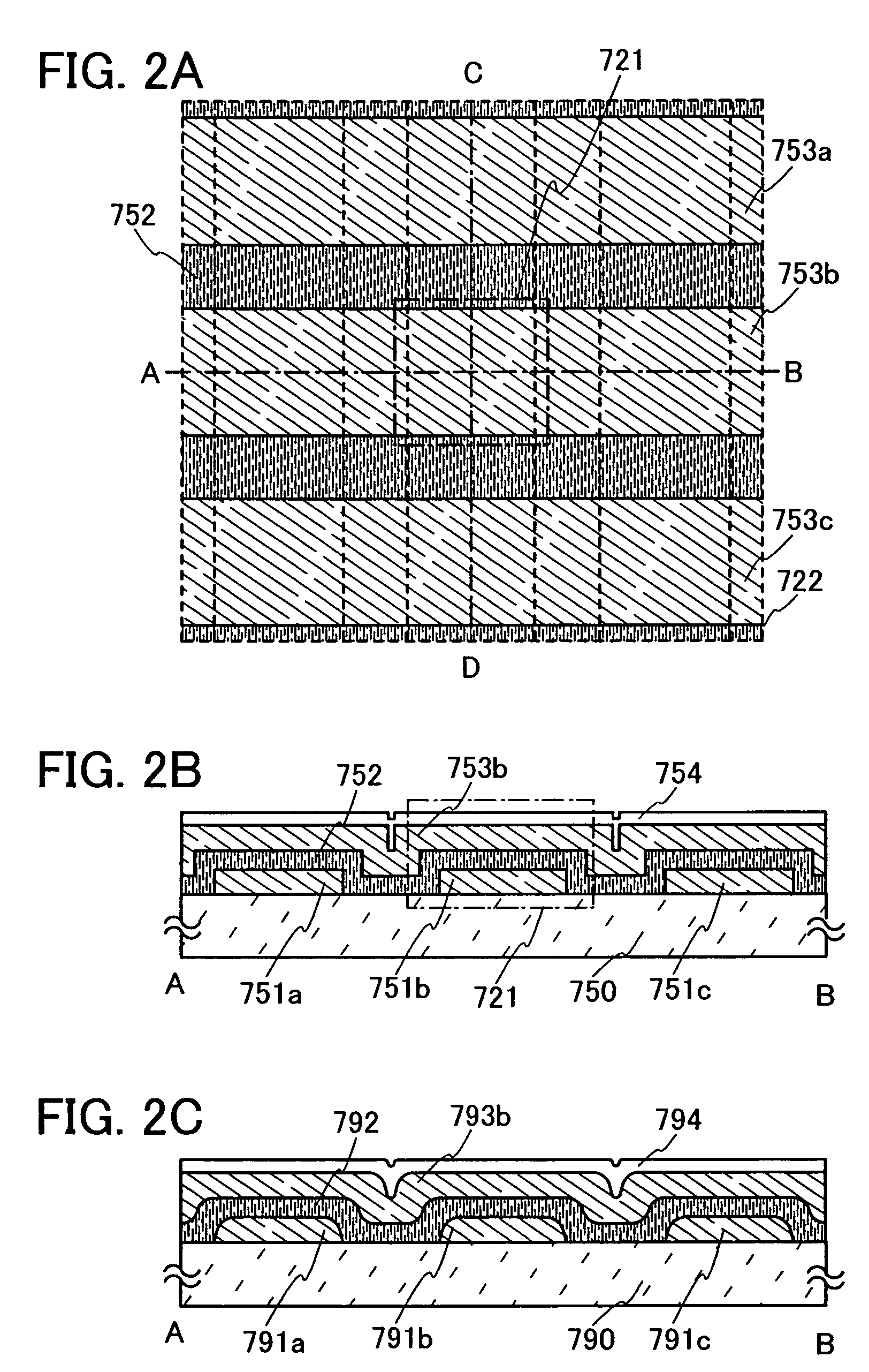
[0115]In this embodiment mode, one structural example of the memory element included in the semiconductor device of the present invention will be described using the drawings. In particular, the case where the semiconductor device is a passive matrix type will be described.

[0116]The memory element of the present invention and an operation mechanism thereof are described using FIGS. 2A to 2C, 6A, and 6B. The memory element in this embodiment mode can be manufactured by the same material and with the same structure as those in Embodiment Mode 1, and therefore, detailed description of the material or the like is omitted here.

[0117]FIGS. 3A to 3C each show one constitution example of the semiconductor device of the invention, which include a memory cell array 722 including memory cells 721 provided in matrix, a circuit 726 including a reading circuit and a writing circuit, a decoder 724, and a decoder 723. It is to be noted that the constitution of a semiconductor device 716 shown here ...

embodiment mode 3

[0135]In this embodiment mode, a semiconductor device having constitution different from that of Embodiment Mode 2 will be described. In particular, the case where the semiconductor device is an active matrix type will be described. A memory element in this embodiment mode can be manufactured by using the same material and with the same structure as that in Embodiment Mode 1, and therefore, detailed description of the material or the like is omitted here.

[0136]FIGS. 5A to 5C show one constitution example of the semiconductor device of this embodiment mode, which include a memory cell array 232 including memory cells 231 in matrix, a circuit 226, a decoder 224, and a decoder 223. The circuit 226 includes a reading circuit and a writing circuit. It is to be noted that the constitution of a semiconductor device 217 shown here is only one example; the semiconductor device may include another circuit such as a sense amplifier, an output circuit, or a buffer, and the writing circuit may b...


PUM

PropertyMeasurementUnit
thicknessaaaaaaaaaa
thicknessaaaaaaaaaa
thicknessaaaaaaaaaa

Abstract

To provide a semiconductor device which is higher functional and reliable and a technique capable of manufacturing the semiconductor device with a high yield at low cost without complexing the apparatus or process. At least one of a first conductive layer and a second conductive layer is formed containing one kind or plural kinds of indium, tin, lead, bismuth, calcium, manganese, or zinc; or oxidation treatment is performed at least one of interfaces between an organic compound layer and the first conductive layer and between the organic compound layer and the second conductive layer. The first conductive layer, the organic compound layer, and the second conductive layer which are formed over a first substrate with a peeling layer interposed therebetween can be peeled from the first substrate with the peeling layer, and transposed to a second substrate.

Description

TECHNICAL FIELD[0001]The present invention relates to a semiconductor device and a manufacturing method of the semiconductor device.BACKGROUND ART[0002]Recently, an individual-recognition technique has drawn attention, in which by giving an ID (individual identification number) to each object, information such as a history of the object is clarified for manufacturing, management, or the like. In particular, a semiconductor device capable of non-contact data transmission and reception has been developed. As such a semiconductor device, an RFID (Radio Frequency Identification: also called an ID tag, an IC tag, an IC chip, an RF (Radio Frequency) tag, a wireless tag, an electronic tag, or a wireless chip) or the like specifically begins to be introduced into companies, markets, or the like.[0003]Such a semiconductor device generally includes an antenna and a circuit (hereinafter, also referred to as an IC (Integrated Circuit) chip) using a semiconductor substrate of silicon (Si) or the...

Claims


Application Information

Patent Timeline
Patent Type & Authority Patents(United States)
IPC IPC(8): H01L21/00
CPCB82Y10/00G11C13/0014H01L27/1214H01L27/1266H01L27/281H01L29/458H01L51/003G02F2001/13613G11C13/00G11C2213/77H01L2251/558G11C2213/79G02F1/13613H10K19/201H10K71/80H10K2102/351
Inventor KUSUMOTO, NAOTOOHSAWA, NOBUHARUYUKAWA, MIKIODOZEN, YOSHITAKA
Owner SEMICON ENERGY LAB CO LTD
Why Eureka
Try Eureka