

Wafer polishing apparatus and method for polishing wafers
a wafer polishing and apparatus technology, applied in the direction of grinding machines, manufacturing tools, lapping machines, etc., can solve the problems of long polishing time, high production cost, complicated polishing process, etc., to reduce equipment and polishing materials, reduce production cost, and reduce the effect of coarse bump removal
Active Publication Date: 2010-05-18
SUMCO CORP
View PDF28 Cites 0 Cited by
- Summary
- Abstract
- Description
- Claims
- Application Information
AI Technical Summary
Benefits of technology
The present invention is a wafer polishing apparatus that can efficiently remove both long wavelength components and short wavelength components in the surface roughness components of wafers and achieve smooth mirror-finished surfaces with no strain. The apparatus includes a polishing plate with a polishing pad, a carrier plate that slides and presses wafers against the polishing pad, and an abrasive slurry supply device that supplies different abrasive slurries with different average grain sizes. The abrasive slurry supply device can change the abrasive slurry being supplied and can include two or more abrasive slurry supply sources and supply pipes connected to the sources. The technical effect of the invention is to improve the polishing efficiency and achieve smooth mirror-finished surfaces with no strain.
Problems solved by technology
As a result, the problem arises in which production costs become high.
Therefore, the problem arises in which the polishing process becomes complicated and it takes a long time to polish the wafers.
Method used
View moreImage
Smart ImageViewing Examples


Examples
example
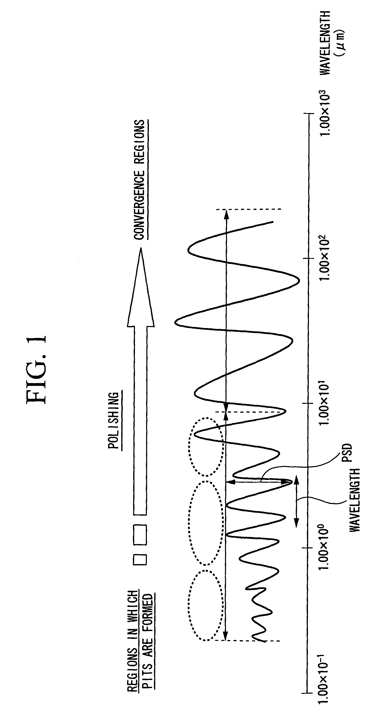
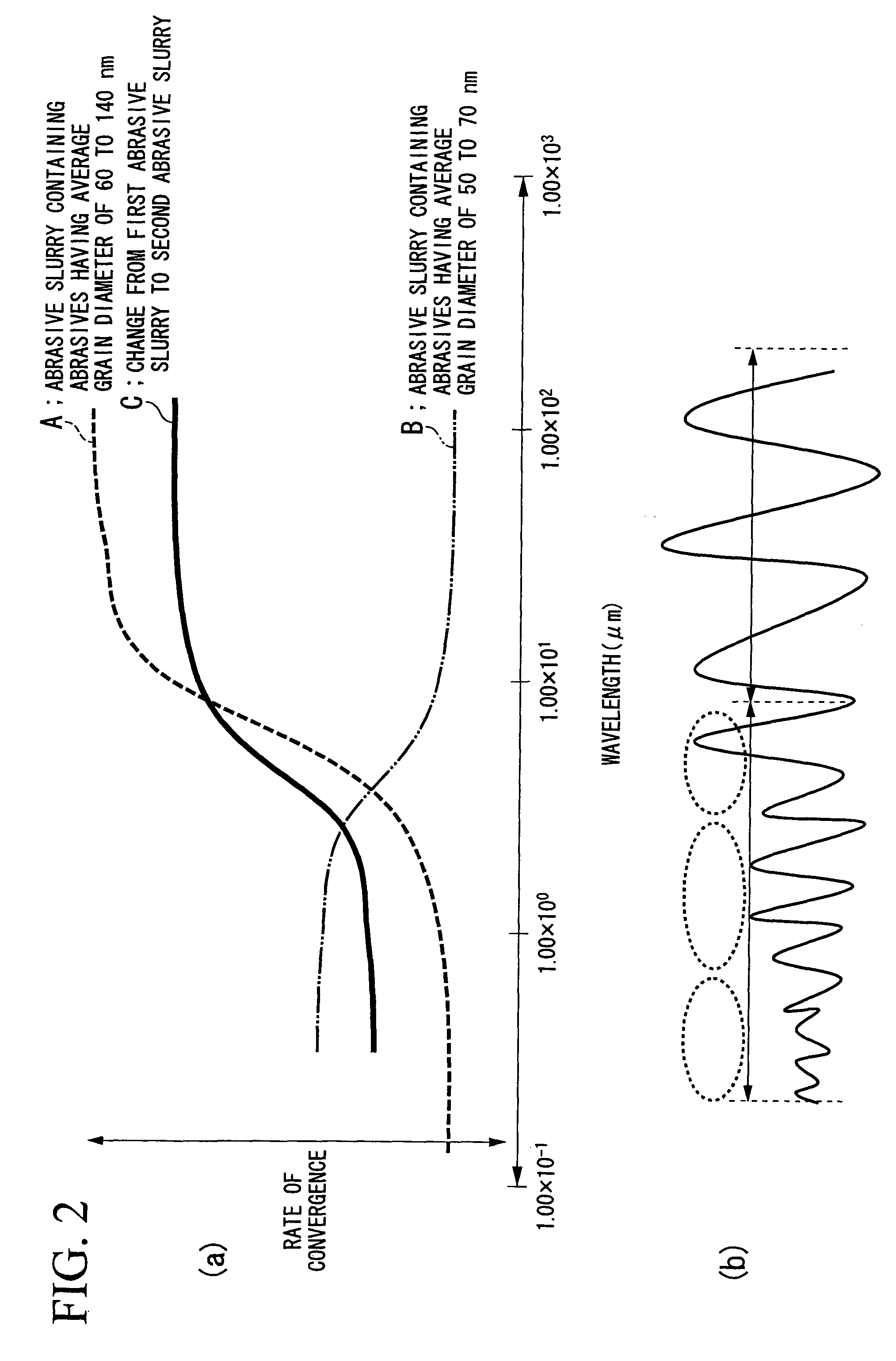
[0061]The wafer polishing apparatus 10 of the present embodiment was used in which the abrasive slurry supply apparatus 16 was provided. As is shown in the embodiment, during the polishing process, the slurry which was supplied to the surface of the polishing pad 11 was changed from a first abrasive slurry which contained the abrasives having a average grain diameter of 60 nm to 140 nm to a second abrasive slurry which contained the abrasives having a average grain diameter of 50 nm to 70 nm, and the surfaces of the silicon wafers W were polished.
Login to View More PUM
| Property | Measurement | Unit |
|---|---|---|
| average grain diameter | aaaaa | aaaaa |
| average grain diameter | aaaaa | aaaaa |
| surface roughness | aaaaa | aaaaa |
Abstract
This wafer polishing apparatus includes: a polishing plate having a polishing pad; a carrier plate which is placed facing the polishing pad and which slides and presses wafers against the polishing pad, while rotating in a state of holding the wafers; and an abrasive slurry supply device, wherein the abrasive slurry supply device is able to supply different abrasive slurries, each of the abrasive slurries contains abrasives of which the average grain size is different from those contained in the other abrasive slurries. This method for polishing wafers includes: while supplying an abrasive slurry to a surface of a polishing pad, sliding and pressing wafers against the polishing pad, wherein different abrasive slurries are supplied to the surface of the polishing pad, and each of the abrasive slurries contains abrasives of which the average grain size is different from those contained in the other abrasive slurries.
Description
BACKGROUND OF THE INVENTION[0001]1. Field of the Invention[0002]The present invention relates to an apparatus for polishing wafers and a method for polishing wafers which are employed to polish surfaces of wafers or the like that forms integrated circuits.[0003]This application claims priority from Japanese Patent Application No. 2005-145612, filed May 18, 2005, the content of which is incorporated herein by reference.[0004]2. Background Art[0005]Generally, a silicon wafer of which the surface has being etched is subjected to a polishing step in which the surface is polished. A conventional polishing includes a first polishing step in which coarse bumps are smoothed away in the surface of the wafer using a wafer polishing apparatus provided with a hard polishing pad and a second polishing step in which eliminates minute pits are eliminated in the surface of the wafer using a wafer polishing apparatus provided with a soft polishing pad. Thereby, the surface of the wafer is finished t...
Claims
Login to View More Application Information
Patent Timeline
 Patent Type & AuthorityPatents(United States)
IPC IPC(8): B24B7/22B24B37/00B24B57/02H01L21/304
CPCB24B37/04H01L21/02024B24B57/02H01L21/304
InventorHASHII, TOMOHIROMURAYAMA, KATSUHIKOKOYATA, SAKAETAKAISHI, KAZUSHIGE
OwnerSUMCO CORP