

Display device and electronic apparatus
a display device and electronic equipment technology, applied in the field of display devices and electronic equipment, can solve the problems of increasing the size of the drive circuit, reducing the yield, increasing manufacturing costs, etc., and achieve the effects of preventing the transfer of heat from each display to the anti-reflective plate, easy joining, and enhancing the mechanical strength of each display
- Summary
- Abstract
- Description
- Claims
- Application Information
AI Technical Summary
Benefits of technology
Problems solved by technology
Method used
Image

Examples
first embodiment
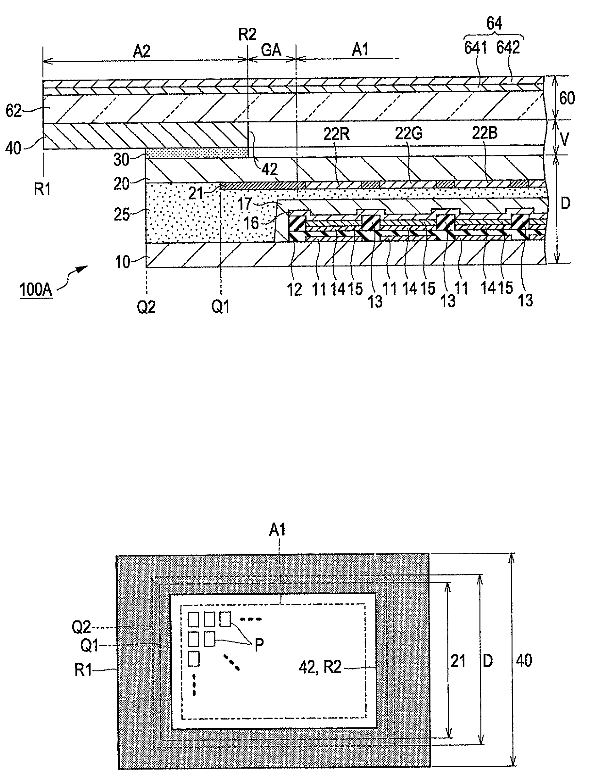
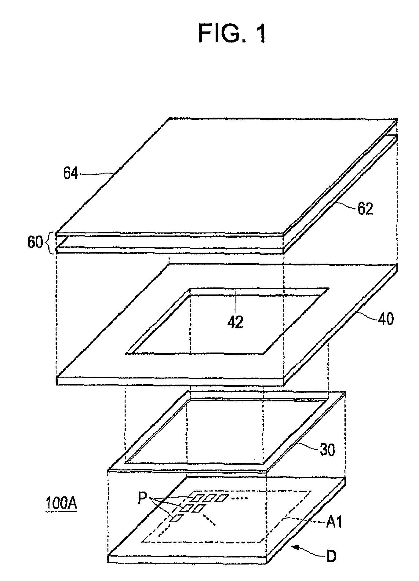
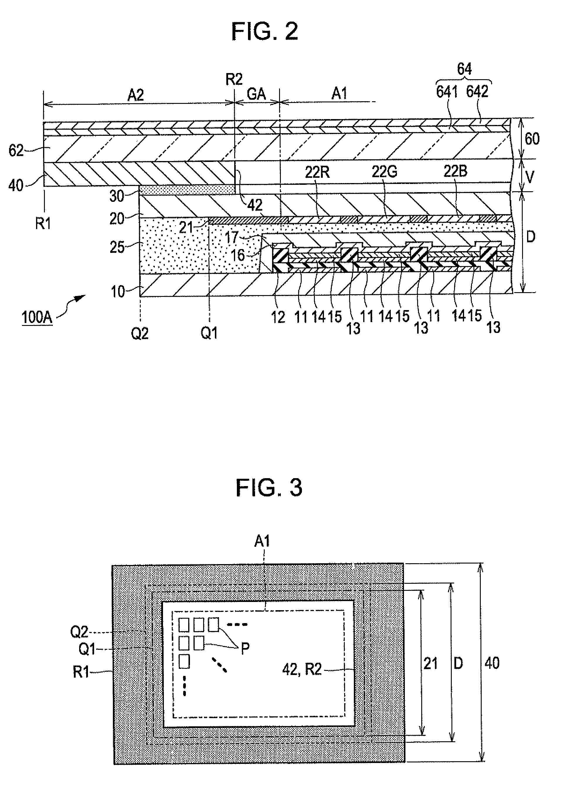
[0042]FIG. 1 is an exploded perspective view of a display device 100A according to a first embodiment of the present invention. FIG. 2 is a cross-sectional view of the display device 100A. Referring to FIGS. 1 and 2, the display device 100A is a flat assembly including a display D, an exterior 40, and an antireflective plate 60. The display D includes a plurality of pixels P arranged two-dimensionally within a display area A1 and displays various images using the pixels P.
[0043]Referring to FIG. 2, the display D includes a first substrate 10 and a second substrate 20 connected to each other, with a light-transmissive joining layer 25 therebetween. The second substrate 20 is located adjacent to the front (viewing) side of the display D (i.e., adjacent to a viewer who views an image displayed on the display D) above the first substrate 10. On a first surface of the first substrate 10 opposed to the second substrate 20, a plurality of light-reflecting layer segments 11 are arranged in ...
second embodiment
[0061]FIG. 6 is an exploded perspective view of a display device 100B according to a second embodiment of the present invention. Referring to FIG. 6, the display device 100B is a flat assembly including, in series, a first display DA and a second display DB that are disposed in spaced-apart relationship in the same plane, an exterior 40, and an antireflective plate 60. The first and second displays DA and DB each have the same structure as that of the display D according to the first embodiment. The displays DA and DB each display various images using a plurality of pixels P arranged two-dimensionally in a display area A1. In the following description, when it is unnecessary to distinguish between the first display DA and the second display DB, the first and second displays DA and DB will be called “displays D”.
[0062]FIG. 7 is a plan view of the display device 100B and conceptually shows the relationship among respective components of the display device 100B. In FIG. 7, the antirefl...
third embodiment
[0069]A third embodiment of the present invention will now be described. The following description will be made with respect to a structure based on that according to the first embodiment as an example. Third to sixth embodiments may be similarly applied to the display device 100B having a plurality of displays D (DA, DB) according to the second embodiment.
[0070]FIG. 10 is a cross-sectional view of a display device 100C according to a third embodiment of the present invention. Referring to FIG. 10, in the display device 100C, the surface of each light-transmissive component in contact with the air is covered with an antireflection (AR) coating layer 70 (70A, 70B, 70C) for preventing reflection on the surface. More specifically, the AR coating layer 70A is disposed on a first surface of an antireflective plate 60 (or a circular polarizer 64) adjacent to the viewing side of the display device 100C, the AR coating layer 70B is disposed on a second surface of the antireflective plate 60...
PUM
| Property | Measurement | Unit |
|---|---|---|
| wavelength | aaaaa | aaaaa |
| reflectance | aaaaa | aaaaa |
| reflectance | aaaaa | aaaaa |
Abstract
Description
Claims
Application Information