Organic light-emitting diode display device and driving method thereof

a technology of light-emitting diodes and display devices, which is applied in the direction of instruments, computing, electric digital data processing, etc., can solve the problems of low light-emission efficiency of pdp, large power consumption, and difficulty in increasing the dimension screen, so as to achieve the effect of reducing the voltage drop

Active Publication Date: 2010-05-25
LG DISPLAY CO LTD
View PDF2 Cites 25 Cited by
  • Summary
  • Abstract
  • Description
  • Claims
  • Application Information

AI Technical Summary

Benefits of technology

[0023]The present embodiments may obviate one or more of the limitations of the related art. For example, in one embodiment, an organic light-emitting diode display device is adaptive to minimize a voltage drop by a driving voltage supply line and an adverse effect by a threshold voltage change of a thin film transistor to uniform display brightness.

Problems solved by technology

However, the PDP has low light-emission efficiency and large power consumption.
The active matrix LCD employing a thin film transistor (hereinafter, referred to as “TFT”) as a switching device has drawbacks in that it is difficult to increase the dimension screen because a semiconductor process is used.

Method used


Image

  • Organic light-emitting diode display device and driving method thereof
  • Organic light-emitting diode display device and driving method thereof
  • Organic light-emitting diode display device and driving method thereof

Examples


first embodiment

[0042]In a first embodiment, as shown in FIG. 5 to FIG. 8, an organic light-emitting diode display device includes a display panel 50 provided m×n pixels 54, a data driver 52 supplying a data voltage to data lines DL1 to DLm, a scan driver 53 sequentially supplying an inverse-phase scanning pulse pair to m scan electrode pairs (E1 to En and S1 to Sn) and a timing controller 51 controlling the drivers 52 and 53.

[0043]In the display panel 50, pixels 54 are formed at pixel areas defined by an intersection of n first and second scan lines (E1 to En and S1 to Sn) and m data lines DL1 to DLm. Signal lines supplying a reference voltage Vref of a constant-voltage, a reference current Iref of a constant-current and a high-level electric potential driving voltage VDD to the pixels 54 are formed at the display panel 50.

[0044]The data driver 52 converts a digital video data RGB from the timing controller 51 into an analog gamma compensation voltage. The data driver 52 supplies an analog gamma c...

second embodiment

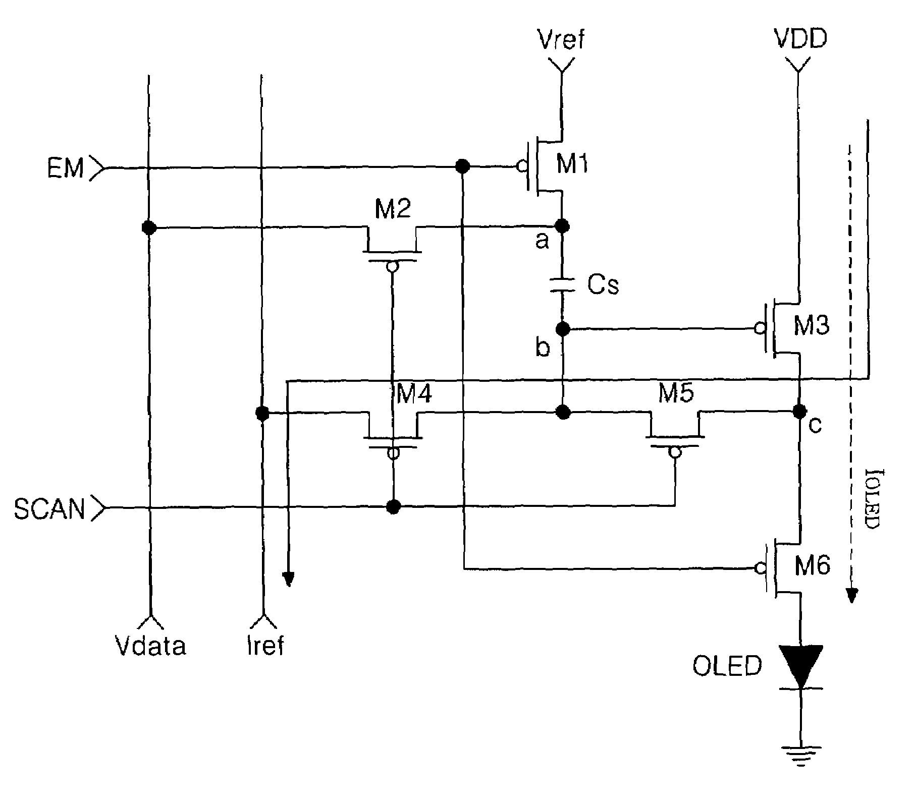
[0071]FIG. 8 shows the pixels 54 at the organic light-emitting diode display device.

[0072]In one embodiment, as shown in FIG. 8, each of the pixels 54 includes the first to sixth TFT M1 to M6, the storage capacitor Cs and the organic light-emitting diode element OLED. The TFTs M1 to M6 are implemented in a p-type MOS-FET. Since the first to fifth TFT M1 to M5, the storage capacitor Cs and the organic light-emitting diode element OLED are identical to those described in the embodiment of the above-mentioned FIG. 6, a detailed explanation as to it will be omitted.

[0073]The third TFT M3 is operated by a diode to flow a reference current Iref during the programming period PP like the above-mentioned embodiment.

[0074]The sixth TFT M6 is connected to a backward diode by the fifth TFT M5 turned-on during the programming period PP to cut-off a current IOLED supplied to the organic light-emitting diode element OLED while forms a current path between the c-node and the organic light-emitting ...


PUM


Abstract

An organic light-emitting diode display device and driving method thereof are provided. The organic light-emitting diode display device including a driving voltage source; a reference voltage source that generates a reference voltage; a reference current source; and a storage capacitor connected between a first node and a second node. An organic light-emitting diode device is connected between a third node and a ground voltage source. A first scanning signal is supplied to a first scan line. A second scanning signal is supplied to a second scan line, the second scanning signal having an inverse-phase against the first scanning signal.

Description

[0001]This application claims the benefit of Korean Patent Application No. P06-0049435 filed in Korea on Jun. 01, 2006, which is hereby incorporated by reference.BACKGROUND[0002]1. Field[0003]The present embodiments relate to an organic light-emitting diode display device and a driving method thereof.[0004]2. Related Art[0005]Recently, various flat panel display devices have been developed. These flat panel display devices have a reduced weight and bulk and are capable of eliminating disadvantages of a cathode ray tube. Such flat panel display devices include, for example, a liquid crystal display device (hereinafter, referred to as “LCD”), a field emission display device (hereinafter, referred to as “FED”), a plasma display panel (hereinafter, referred to as “PDP”) and an electro-luminescence display device.[0006]In such flat panel display devices, the PDP has a light weight, a small bulk size and a large dimension screen because its structure and manufacturing process are simple. ...

Claims


Application Information

Patent Timeline
Patent Type & Authority Patents(United States)
IPC IPC(8): G09G3/30G06F3/038G09G3/32G09G5/00
CPCG09G3/3233G09G2300/0417G09G2320/043G09G2300/0842G09G2300/0861G09G2300/0819G09G3/30
Inventor KIM, O HYUNCHUNG, HOON JUJUNG, MYOUNG HOON
Owner LG DISPLAY CO LTD
Why Eureka
Try Eureka