Contact mapping using channel routing

Inactive Publication Date: 2010-05-25
CIENA
View PDF65 Cites 13 Cited by
  • Summary
  • Abstract
  • Description
  • Claims
  • Application Information

AI Technical Summary

Benefits of technology

[0011]According to the present invention, a technique for improved contact mapping of the contacts of a PLD to one or more other electronic components. In one embodiment, the technique may be realized as a method for mapping contacts of a programmable logic device (PLD) to an electronic component in a signal routing device having one or more layers. The method comprises assigning a set of one or more contacts of the PLD to one or more respective contacts of the electronic component based at least in part on a pattern of electrically conductive traces routed from respective contacts of the electronic component via one or more channels formed at one or more layers of the signal routing device.
[0012]In another embodiment, the technique may be realized as a method for optimizing a mapping of contacts of a programmable logic device (PLD) to contacts of an electronic component in a signal routing device having one or more layers. The method comprises determining a first pattern of electrically conductive traces routed from respective contacts of the electronic component via one or more channels formed at one or more layers of the signal routing device, determining a first contact assignment pattern for one or more contacts of the PLD based at least in part on the first pattern of electrically conductive traces, refining the first pattern of electrically conductive traces based at least in part on the first contact assignment pattern to generate a second pattern of electrically conductive traces routed from the respective contacts of the electronic component via one or more channels formed at one or more layers of the signal routing device

Problems solved by technology

However, with the advent of high-density, multiple layer designs, inefficient mapping of contacts of PLDs to other electronic components, such

Method used


Image

  • Contact mapping using channel routing
  • Contact mapping using channel routing
  • Contact mapping using channel routing

Examples


Embodiment Construction

)

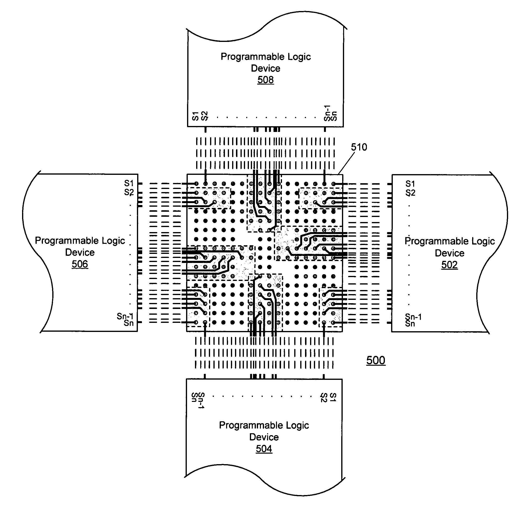
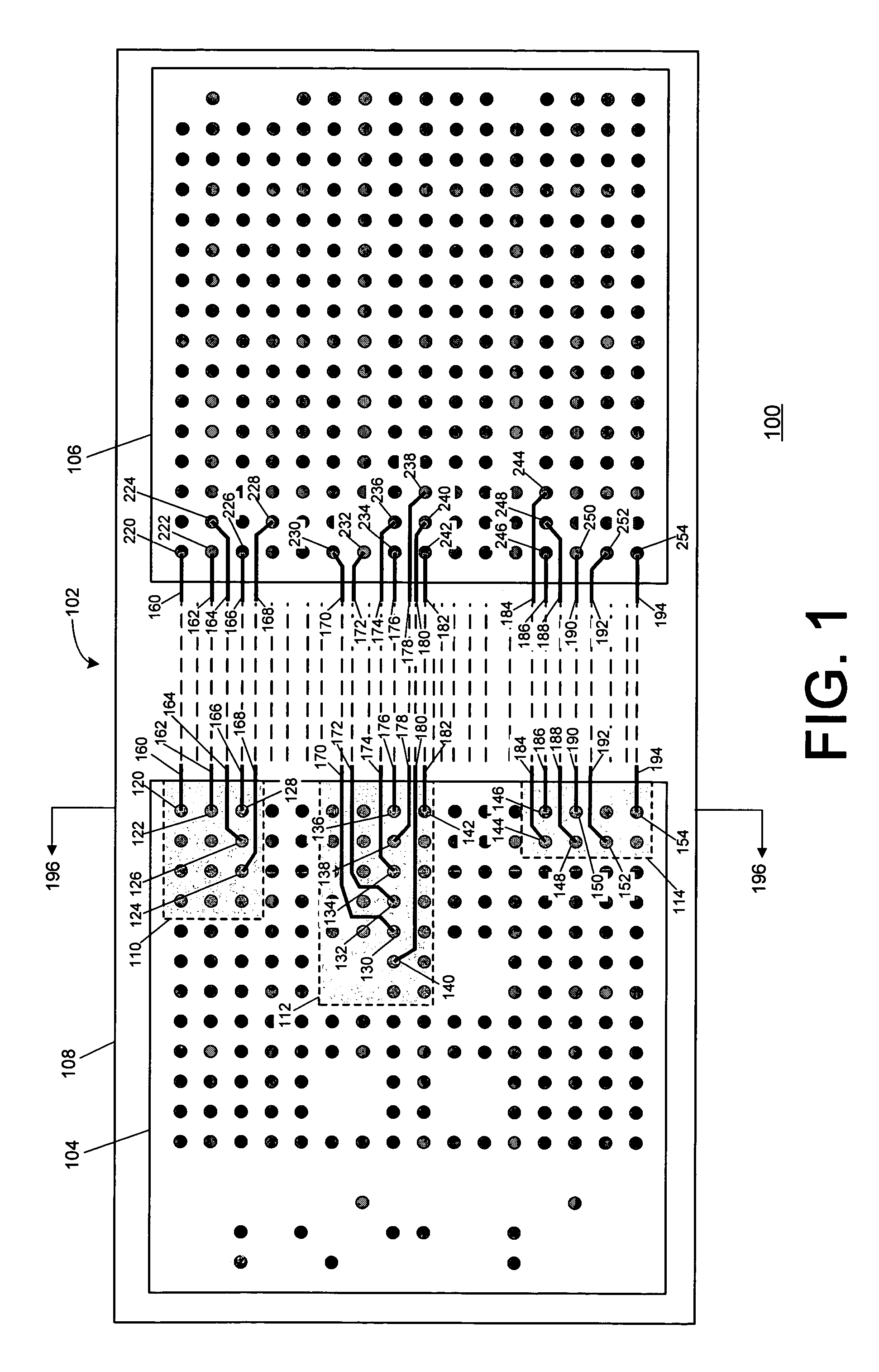
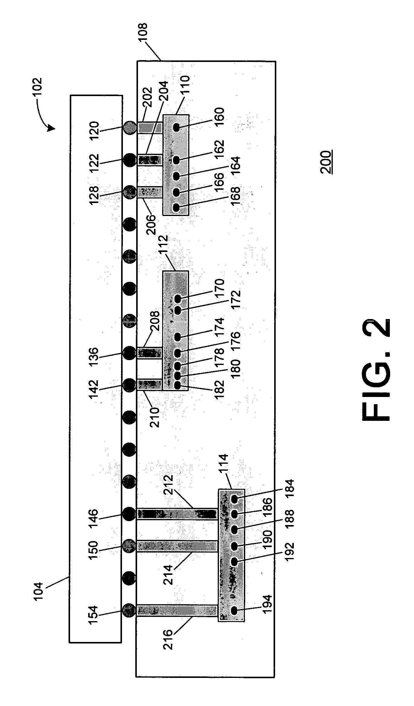
[0023]At the outset, it is helpful to refer to the microvia-based techniques for reducing the number of layers in a multilayer signal routing device and the power / ground-based techniques for reducing the number of layers in a multilayer signal routing device as have been substantially described in the above-referenced U.S. Provisional Patent Application No. 60 / 212,387, the above-referenced U.S. patent application Ser. No. 09 / 651,188, now U.S. Pat. No. 6,388,890, the above-referenced U.S. patent application Ser. No. 10 / 101,211, the above-referenced U.S. patent application Ser. No. 10 / 126,700, now U.S. Pat. No. 6,545,876, the above-referenced U.S. patent application Ser. No. 10 / 326,123, the above-referenced U.S. patent application Ser. No. 10 / 326,079, and the above-referenced U.S. patent application Ser. No. 10 / 407,460, all of which have been incorporated by reference herein in their entirety. The above-referenced techniques may be used beneficially in conjunction with one or more of...


PUM

PropertyMeasurementUnit
Electrical conductivityaaaaaaaaaa

Abstract

A technique for improved mapping of the contacts of a PLD to the contacts of one or more other electronic components are provided. In one particular exemplary embodiment, the technique may be realized as a method for mapping contacts of a programmable logic device (PLD) to an electronic component in a signal routing device having one or more layers. The method comprises assigning a set of one or more contacts of the PLD to one or more respective contacts of the electronic component based at least in part on a pattern of electrically conductive traces routed from respective contacts of the electronic component via one or more channels formed at one or more layers of the signal routing device.

Description

CROSS-REFERENCE TO RELATED APPLICATIONS[0001]This patent application claims priority to U.S. Provisional Patent Application No. 60 / 475,880, filed Jun. 5, 2003, which is hereby incorporated by reference herein in its entirety.[0002]This patent application is a continuation-in-part patent application of U.S. patent application Ser. No. 10 / 101,211, filed Mar. 20, 2002, which is a continuation-in-part patent application of U.S. patent application Ser. No. 09 / 651,188, filed Aug. 30, 2000, now U.S. Pat. No. 6,388,890, which claims priority to U.S. Provisional Patent Application No. 60 / 212,387, filed Jun. 19, 2000, all of which are hereby incorporated by reference herein in their entirety.[0003]This patent application is also a continuation-in-part patent application of U.S. patent application Ser. No. 10 / 326,123, filed Dec. 23, 2002, which is a continuation-in-part patent application of the above-referenced U.S. patent application Ser. No. 10 / 101,211, and a continuation-in-part patent app...

Claims


Application Information

Patent Timeline
IPC IPC(8): G06F17/50H05K3/02
CPCH05K3/0005H05K1/0286H05K1/0298Y10T29/49155H05K2201/10689Y10T29/49156H05K2201/10212
Inventor KWONG, HERMANSOH, KAH MINGHANDFORTH, MARTINMARCANTI, LARRY
Owner CIENA
Why Eureka
Try Eureka