Method, system and computer-readable code for testing of flash memory

a flash memory and test method technology, applied in the field of flash memory device manufacture, can solve the problems of poor performance, lower reliability of mbc than sbc, and drawbacks of using mbc flash

Inactive Publication Date: 2010-06-01
WODEN TECH INC
View PDF20 Cites 17 Cited by
  • Summary
  • Abstract
  • Description
  • Claims
  • Application Information

AI Technical Summary

Benefits of technology

[0022]It is noted that device testing is an important stage of manufacturing, and that methods, systems and devices provided by certain embodiments of the present invention are useful for reducing the cost of device manufacturing in general, and the testing phase of device manufacturing in particular.

Problems solved by technology

However, there are drawbacks to using MBC flash.
Average read and write times of MBC memories are longer than of SBC memories, resulting in worse performance.
Also, the reliability of MBC is lower than SBC.
Thus, a disturbance in the threshold voltage (e.g. leakage of stored charge causing a threshold voltage drift or interference from operating neighboring cells) that are insignificant in SBC because of the large gap between the two states, may cause an MBC cell to move from one state to another, resulting in an erroneous bit.
The end result is a lower performance specification of MBC cells in terms of data retention time or the endurance of the device to many write / erase cycles.
Another ramification of the lower reliability of MBC devices compared to SBC devices is the required level of error correction.
One reason for this is that the flash device might have bad blocks that should not be used.
A given flash memory die may be subjected to other tests, but the testing for bad blocks is typically the most time consuming.
Then if some of the memory dies are found defective at the MCP-stage testing, those MCP devices have to be scrapped.
This causes the loss of not only the memory die (that would have been scrapped anyway), but also the expensive microprocessor die and the cost of packaging.
However, manufacturing KGD flash memory dies is not simple.
The test equipment used for the wafer sorting stage is complex and expensive, using such equipment for long tests makes the costs of testing high.
Also, bad blocks testing is not well suited for execution of the tests on many dies in parallel at the wafer sort stage.
This further complicates bad blocks testing at wafer sort stage and makes it more costly.
One other factor is even more significant in further increasing the costs of bad blocks testing at wafer sort stage.
This further increases the costs of the testing equipment and consequently the testing costs per die.
However, even if packaged in a convenient package, testing of NAND flash devices for bad blocks is quite an expensive task.
The reason for this is that due to the requirement for separate handling of each device (as explained above) the testing should be performed using expensive memory testers, which are capable of testing only a limited number of devices at the same time (typically about 100), and since the test time for each device is significant, so is the cost of testing.
This is especially true for bad blocks testing.
Bad blocks testing requires many such operations, as typically each page in the device is written multiple times during the test.
With the increased use of MBC devices, this implies that costs of flash testing are increasing.

Method used


Image

  • Method, system and computer-readable code for testing of flash memory
  • Method, system and computer-readable code for testing of flash memory
  • Method, system and computer-readable code for testing of flash memory

Examples


Embodiment Construction

[0053]The present invention will now be described in terms of specific, example embodiments. It is to be understood that the invention is not limited to the example embodiments disclosed. It should also be understood that not every feature of the methods of flash memory device manufacturing, systems for testing flash memory devices and flash memory devices described is necessary to implement the invention as claimed in any particular one of the appended claims. Various elements and features of devices are described to fully enable the invention. It should also be understood that throughout this disclosure, where a process or method is shown or described, the steps of the method may be performed in any order or simultaneously, unless it is clear from the context that one step depends on another being performed first.

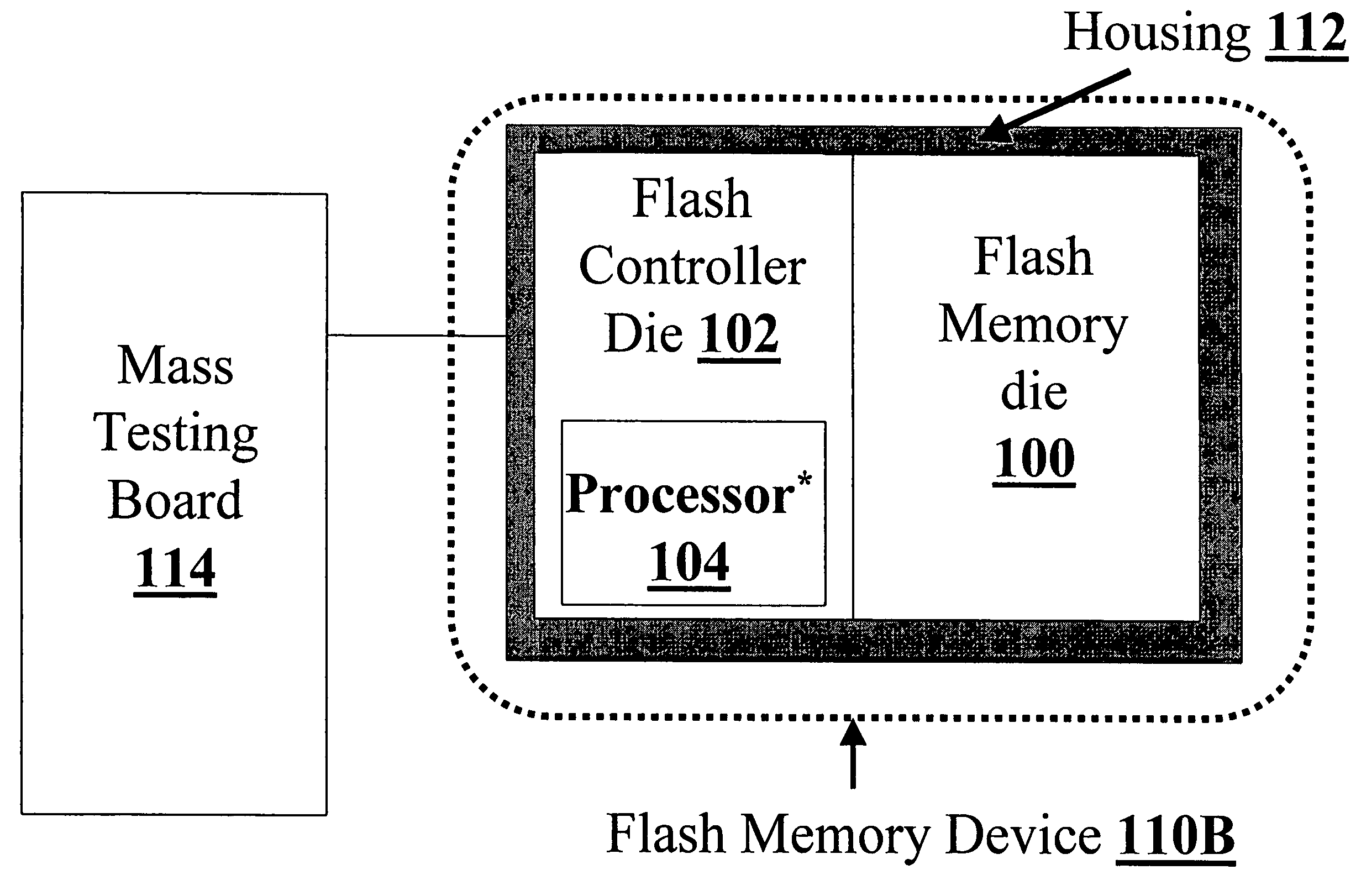
Flash Memory Device 110 and the Testing System

[0054]Referring to FIG. 3, it is noted that embodiments of the present invention relate to the testing of flash memory dies ...


PUM


Abstract

Methods, systems and devices for testing flash memory dies are disclosed. According to some embodiments, during the post-wafer sort stage of device manufacture, a plurality of flash memory devices, each of which includes a flash controller die and at least one flash memory die associated with a common housing, are subjected to a testing process, for examples, a batch testing process or a mass testing process. During testing, a respective flash controller residing on a respective flash controller die executes at least one test program to test one or more respective flash memory dies of the respective flash device. A testing system including at least 100 of the flash memory devices and a mass-testing board is disclosed. Furthermore, flash memory devices where the flash controller is operative to test one or more of the flash memory dies are disclosed. Exemplary testing includes but is not limited to bad block testing.

Description

CROSS-REFERENCE TO RELATED APPLICATIONS[0001]This patent application claims the benefit of U.S. Provisional Patent Application No. 60 / 731,921, filed Nov. 1, 2005 by the present inventors, and is a continuation-in-part of U.S. patent application Ser. No. 10 / 697,981, filed Oct. 31, 2003 now U.S. Pat. No. 7,424,659, by one of the present inventors.FIELD OF THE INVENTION[0002]The present invention relates to the manufacture of flash memory devices in general, and to the testing of flash memory dies during manufacture in particular.BACKGROUNDSingle Bit and Multi-Bit Flash Memory Cells[0003]Flash memory devices have been known for many years. Typically, each memory cell within a flash memory device stores one bit of information. The traditional way to store a bit in a flash memory cell has been by supporting two states of the memory cell. One state represents a logical “0” and the other state represents a logical “1”.[0004]In a flash memory cell, the two states are implemented by having a...

Claims


Application Information

Patent Timeline
Patent Type & Authority Patents(United States)
IPC IPC(8): G11C29/00G11C7/00
CPCG11C11/5621G11C29/16G11C2029/0401G11C16/04
Inventor MURIN, MARKLASSER, MENAHEMMEIR, AVRAHAM
Owner WODEN TECH INC
Why Eureka
Try Eureka