Eureka AIR delivers breakthrough ideas for toughest innovation challenges, trusted by R&D personnel around the world.

Multi-plasma neutral beam source and method of operating

a beam source and neutron technology, applied in the direction of optical radiation measurement, instruments, spectrometry/spectrophotometry/monochromators, etc., can solve the problems of electrically charged particles, semiconductor device manufacturing, and semiconductor structure toleran

Active Publication Date: 2010-06-08
TOKYO ELECTRON LTD
View PDF10 Cites 30 Cited by
  • Summary
  • Abstract
  • Description
  • Claims
  • Application Information

AI Technical Summary

Benefits of technology

The invention is about a method and system for using a neutral beam source to treat a substrate. The neutral beam source creates a beam of neutral particles that can be used for semiconductor processing applications, such as etching. The processing system includes a beam chamber, a plasma generation system, a plasma heating system, an electron acceleration member, a neutralizer grid, and a pumping system. The neutral beam source is coupled to a process chamber where the substrate is placed for treatment. The method involves forming the neutral beam, pumping the processing space, and exposing the substrate to the neutral beam. The technical effect of this invention is to provide a more efficient and effective way to treat substrates with a neutral beam source.

Problems solved by technology

However, the use of plasma (i.e., electrically charged particles), itself, produces problems in the manufacture of semiconductor devices.
Therefore, the tolerance of semiconductor structures for the charge carried by particles impinging on them during the manufacturing process, such as a dry plasma etching process, has become quite limited and the structures for dissipating such charges during manufacture are sometimes required, often complicating the design of the semiconductor device.
Even then, the trajectory may be altered and the flux of a neutral beam can be severely depleted by collisions with other particles which may or may not have been neutralized and which may have trajectories which are not precisely parallel.

Method used


Image

  • Multi-plasma neutral beam source and method of operating
  • Multi-plasma neutral beam source and method of operating
  • Multi-plasma neutral beam source and method of operating

Examples


Embodiment Construction

[0024]In the following description, to facilitate a thorough understanding of the invention and for purposes of explanation and not limitation, specific details are set forth, such as a particular geometry of the neutral beam source and the processing system and various descriptions of the system components. However, it should be understood that the invention may be practiced with other embodiments that depart from these specific details.

[0025]Nonetheless, it should be appreciated that, contained within the description are features which, notwithstanding the inventive nature of the general concepts being explained, are also of an inventive nature.

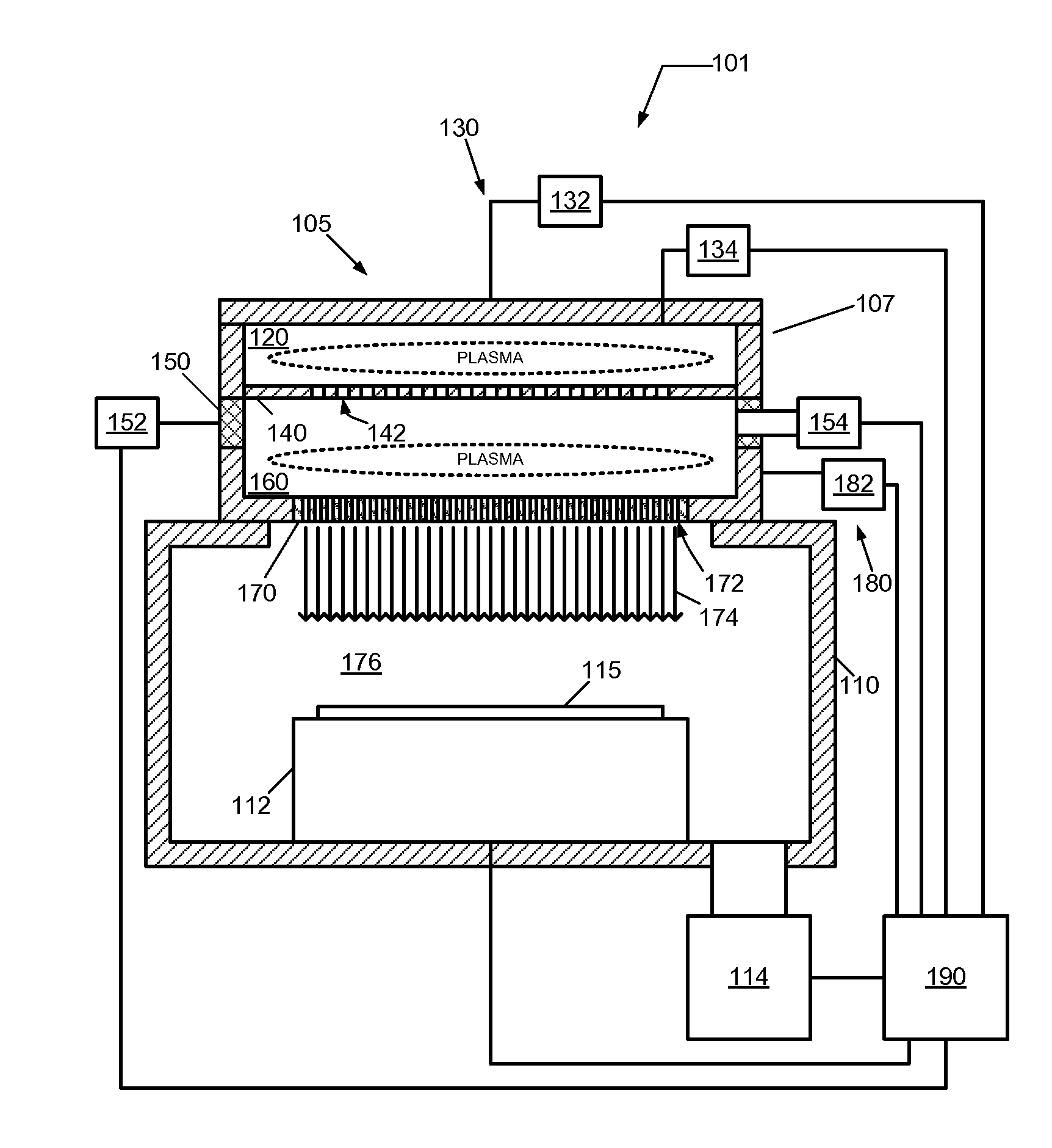
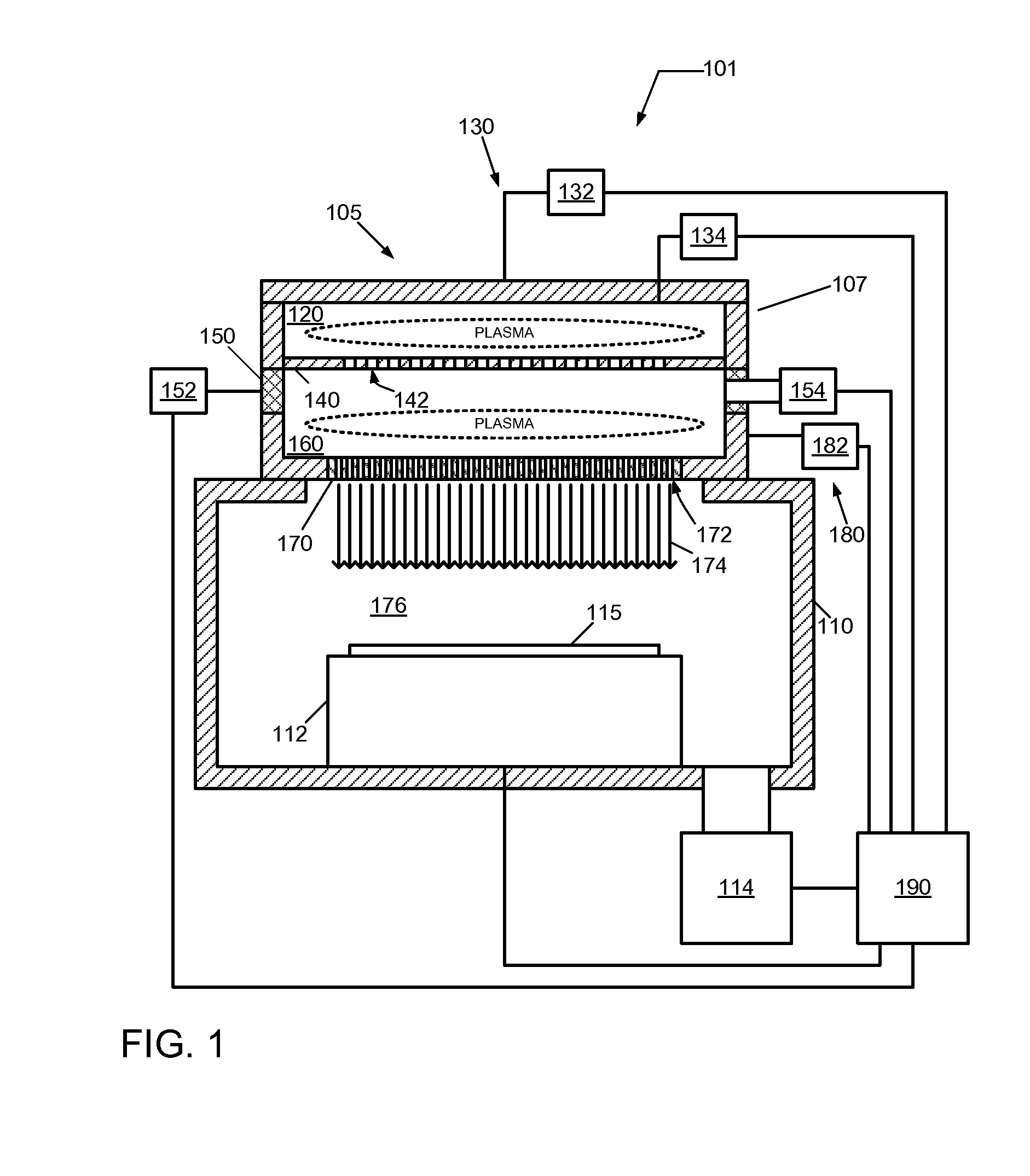
[0026]Referring now to the drawings, wherein like reference numerals designate identical or corresponding parts throughout the several views, FIG. 1 depicts a processing system 101 comprising a neutral beam source 105 configured to produce a neutral beam 174, and a process chamber 110 configured to provide a contaminant-free, vacuum environ...


PUM

PropertyMeasurementUnit
DC voltageaaaaaaaaaa
breakdown voltagesaaaaaaaaaa
frequencyaaaaaaaaaa

Abstract

Method and system for producing a neutral beam source is described. The neutral beam source comprises a plasma generation system for forming a first plasma in a first plasma region, a plasma heating system for heating electrons from the first plasma region in a second plasma region to form a second plasma, and a neutralizer grid for neutralizing ion species from the second plasma in the second plasma region. Furthermore, the neutral beam source comprises an electron acceleration member configured to accelerate the electrons from the first plasma region into the second plasma region. Further yet, the neutral beam source comprises a pumping system that enables use of the neutral beam source for semiconductor processing applications, such as etching processes.

Description

CROSS-REFERENCE TO RELATED APPLICATIONS[0001]This application is related to pending U.S. patent application Ser. No. 11 / 869,656, entitled “NEUTRAL BEAM SOURCE AND METHOD FOR PLASMA HEATING”, filed on Oct. 9, 2007. The entire content of this application is herein incorporated by reference in its entirety.BACKGROUND OF THE INVENTION[0002]1. Field of the Invention[0003]The invention relates to a method and system for operating a neutral beam source for treating a substrate and, more particularly, to a method and system for creating a neutral beam and pumping a processing system utilizing a neutral beam source.[0004]2. Description of Related Art[0005]During semiconductor processing, plasma is often utilized to assist etch processes by facilitating the anisotropic removal of material along fine lines or within vias (or contacts) patterned on a semiconductor substrate. Furthermore, plasma is utilized to enhance the deposition of thin films by providing improved mobility of adatoms on a se...

Claims


Application Information

Patent Timeline
Patent Type & Authority Patents(United States)
IPC IPC(8): H05H3/06H05H3/00
CPCH01J37/32357H05H3/02H01J37/32422
Inventor CHEN, LEEFUNK, MERRITT
Owner TOKYO ELECTRON LTD
Why Eureka
Eureka Blog
Learn More