Printed circuit board having vias

a technology of printed circuit boards and vias, which is applied in the direction of printed circuit manufacturing, cross-talk/noise/interference reduction, printed circuit aspects, etc., can solve the problems of reducing the quality of signals, affecting the integrity of signals, and reflection of output signals, so as to reduce the reflection of input signals

Inactive Publication Date: 2010-06-29
HONG FU JIN PRECISION IND (SHENZHEN) CO LTD +1
View PDF7 Cites 1 Cited by
  • Summary
  • Abstract
  • Description
  • Claims
  • Application Information

AI Technical Summary

Benefits of technology

[0010]Commonly in the design process, diameters of the pad and the anti-pad of the via are reduced simultaneously. Thereby, the reflection of the input signals is reduced because of a reduction in a capacitance of the corresponding pad. However, the diameter of the pad connected with the output signals is reduced as well, which results in a reduction in reflection of the output signals, therefore, the error of the output signals is larger which affects the signal integrity of the output signals. When the signals are transmitted, the capacitance of the pad connected with the input signal lines is large, so the impedance of the pad is small nearly to the point of being a short circuit, however, the signal lines have a certain impedance. Therefore, the impedance of the transmission lines are discontinuous, and large reflections are caused.

Problems solved by technology

However, qualities of signals are often reduced because of signal reflection that is caused by discontinuity of impedance in transmission lines of the PCB.
When a connection between the vias and transmission lines is necessary, discontinuity of impendence of transmission lines affects the integrity of the signals.
However, the diameter of the pad connected with the output signals is reduced as well, which results in a reduction in reflection of the output signals, therefore, the error of the output signals is larger which affects the signal integrity of the output signals.
Therefore, the impedance of the transmission lines are discontinuous, and large reflections are caused.

Method used


Image

  • Printed circuit board having vias
  • Printed circuit board having vias
  • Printed circuit board having vias

Examples


Embodiment Construction

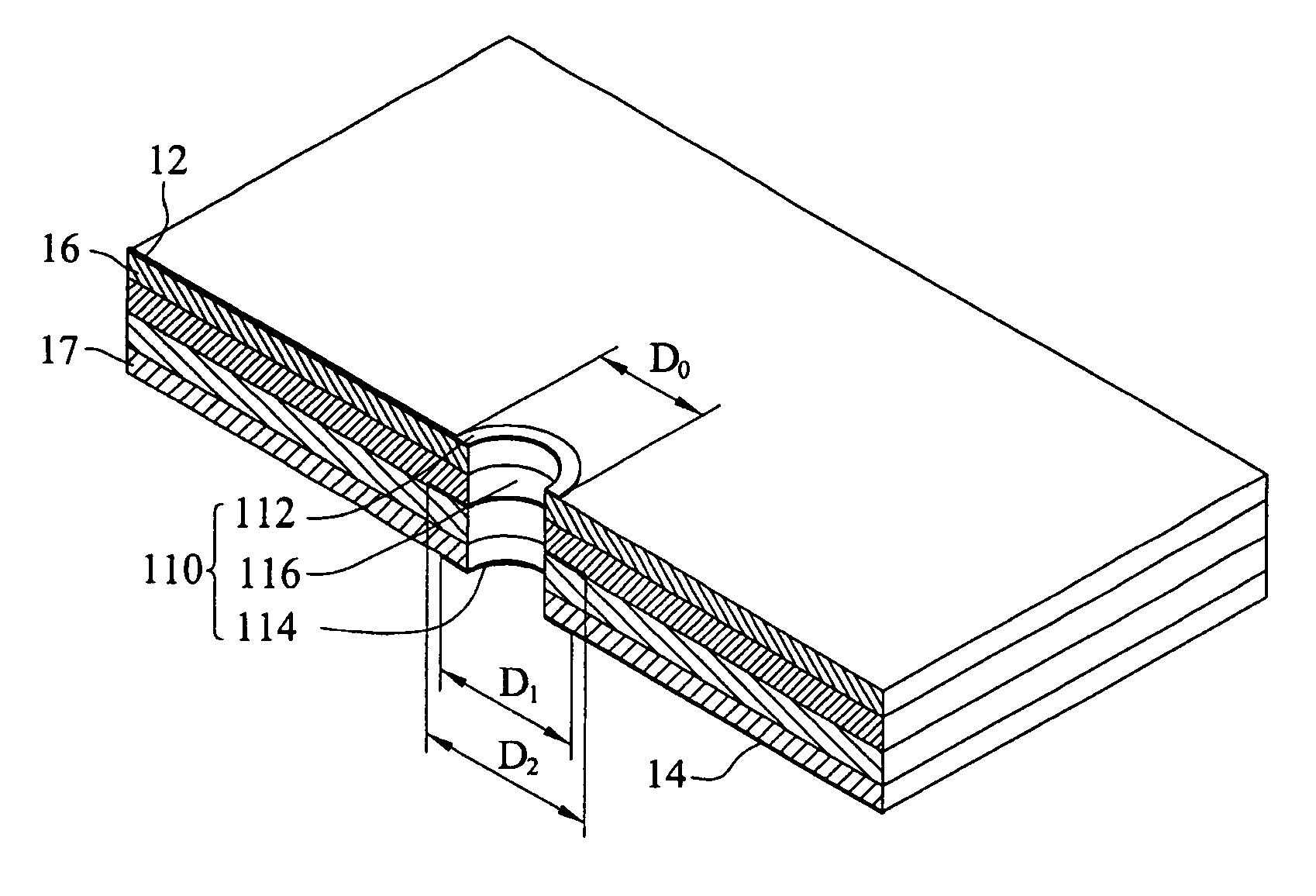
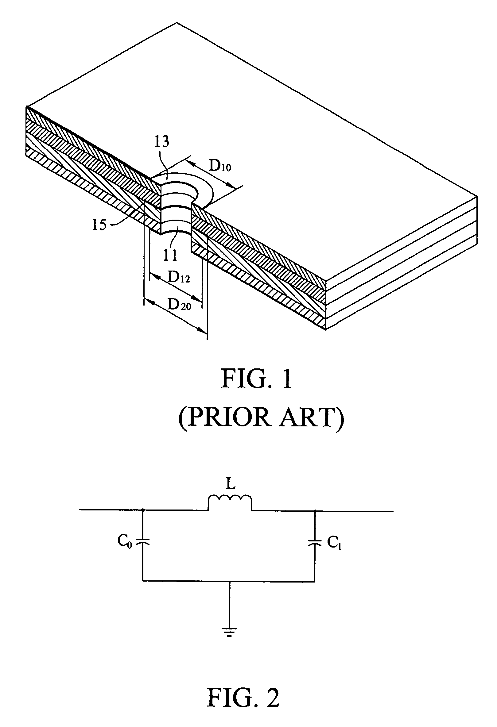
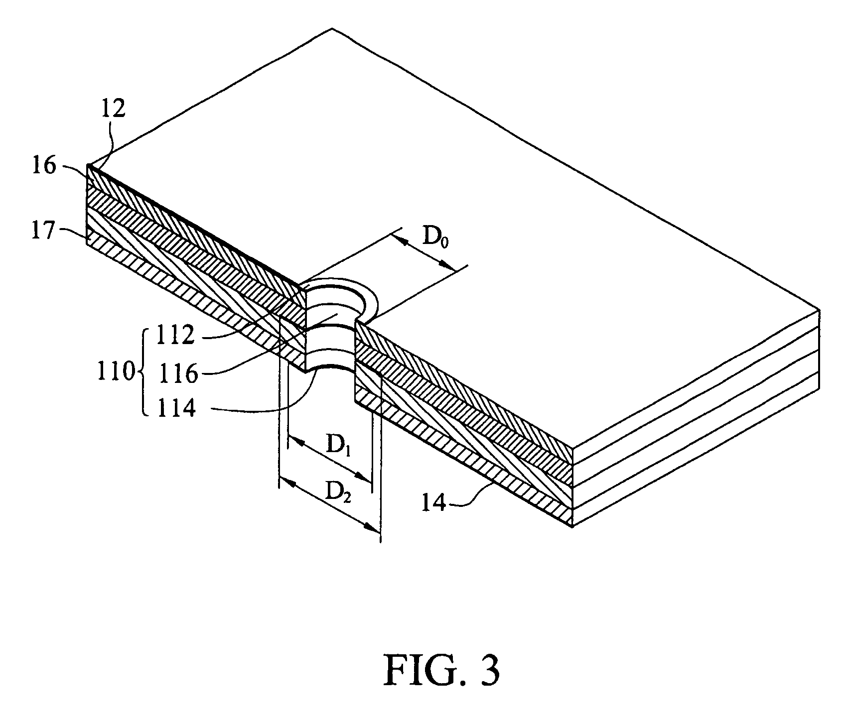
[0019]Referring to FIG. 3, a circuit assembly like a PCB having vias in accordance with a preferred embodiment of the present invention includes a first signal layer 16, a second signal layer 17, a via 110, an input signal line 12, and an output signal line 14. The via 110 includes a drill hole 116, a first pad 112 connected to the first signal layer 16 and encircling an end of the drill hole 116 is electrically connected with the input signal line 12, and a second pad 114 connected to the second layer 17 and encircling an other end of the drill hole 116 is electrically connected with the output signal line 14. In the preferred embodiment of the invention, an outer diameter D0 of the first pad 112 is smaller than an outer diameter D1 of the second pad 114, that is, D01. Therefore, an extending length of the first pad 112 away from the drill hole 116 is smaller than an extending length of the second pad 114 away from the drill hole 116. Compared with the conventional technology, the ...


PUM

PropertyMeasurementUnit
reflectionsaaaaaaaaaa
outer diameteraaaaaaaaaa
transmission characteristicsaaaaaaaaaa

Abstract

A printed circuit board (PCB) having vias for reducing reflections of input signals includes a first signal layer, a second signal layer, one via, an input signal line arranged on the first signal layer, and an output signal line arranged on the second signal layer. The via further includes a drill hole, a first pad, and a second pad. The first pad is electrically connected with the input signal line, and the second pad is electrically connected with the output signal line. An outer diameter of the first pad is smaller than an outer diameter of the second pad.

Description

BACKGROUND[0001]1. Field of the Invention[0002]The present invention relates to a printed circuit board (PCB), and more particularly to a PCB having vias for reducing reflections of input signals.[0003]2. General Background[0004]In modern communications, transmission speed of signals has become quicker and quicker. Signal integrity refers to fidelity of signal curves. However, qualities of signals are often reduced because of signal reflection that is caused by discontinuity of impedance in transmission lines of the PCB.[0005]More signal transmission layers are needed because of the increasing density of signal lines. So it is inevitable that the signal transmissions between different layers of a PCB should be achieved through conductive vias. Design of the conductive vias is crucial in the design of multilayer PCBs. The vias can be divided into three types according to their usage and process of manufacture. They are blind vias, buried vias, and through vias. The blind vias are usu...

Claims


Application Information

Patent Timeline
Patent Type & Authority Patents(United States)
IPC IPC(8): H01R12/04H05K1/11H01K3/22
CPCH05K1/0216H05K1/116H05K3/429Y10T29/49165H05K2201/09509H05K2201/09536H05K2201/09718H05K2201/0352
Inventor LIN, YU-HSUYEH, SHANG-TSANGHUANG, CHAO-CHENLI, CHUAN-BING
Owner HONG FU JIN PRECISION IND (SHENZHEN) CO LTD
Why Eureka
Try Eureka