

Determination of film thickness during chemical mechanical polishing
a technology of thickness determination and chemical mechanical polishing, applied in the direction of semiconductor/solid-state device testing/measurement, lapping machines, instruments, etc., can solve the problems of contact alignment, other fabrication problems, and devices that may not act as planned, and achieve high speed.
- Summary
- Abstract
- Description
- Claims
- Application Information
AI Technical Summary
Benefits of technology
Problems solved by technology
Method used
Image

Examples
Embodiment Construction
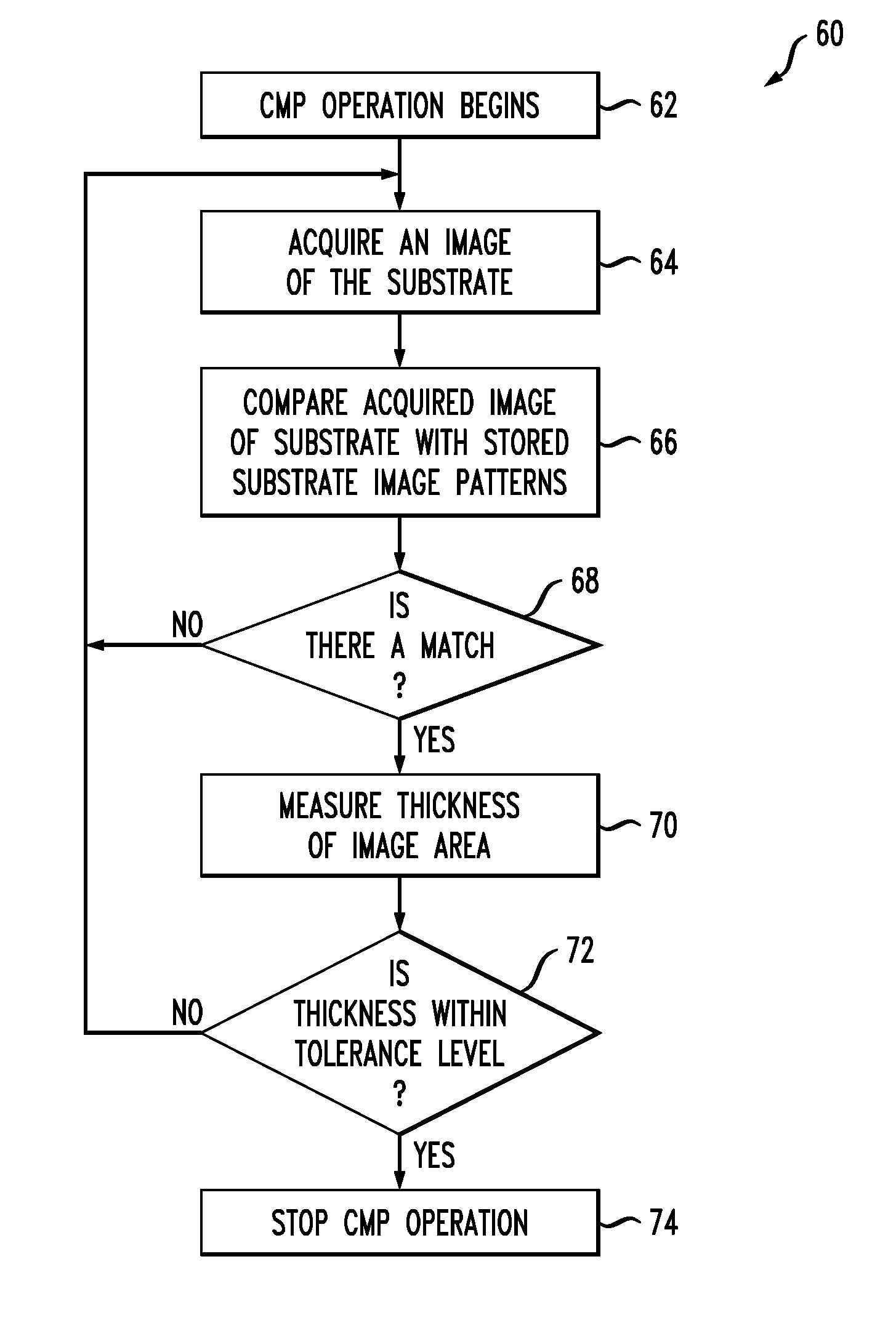
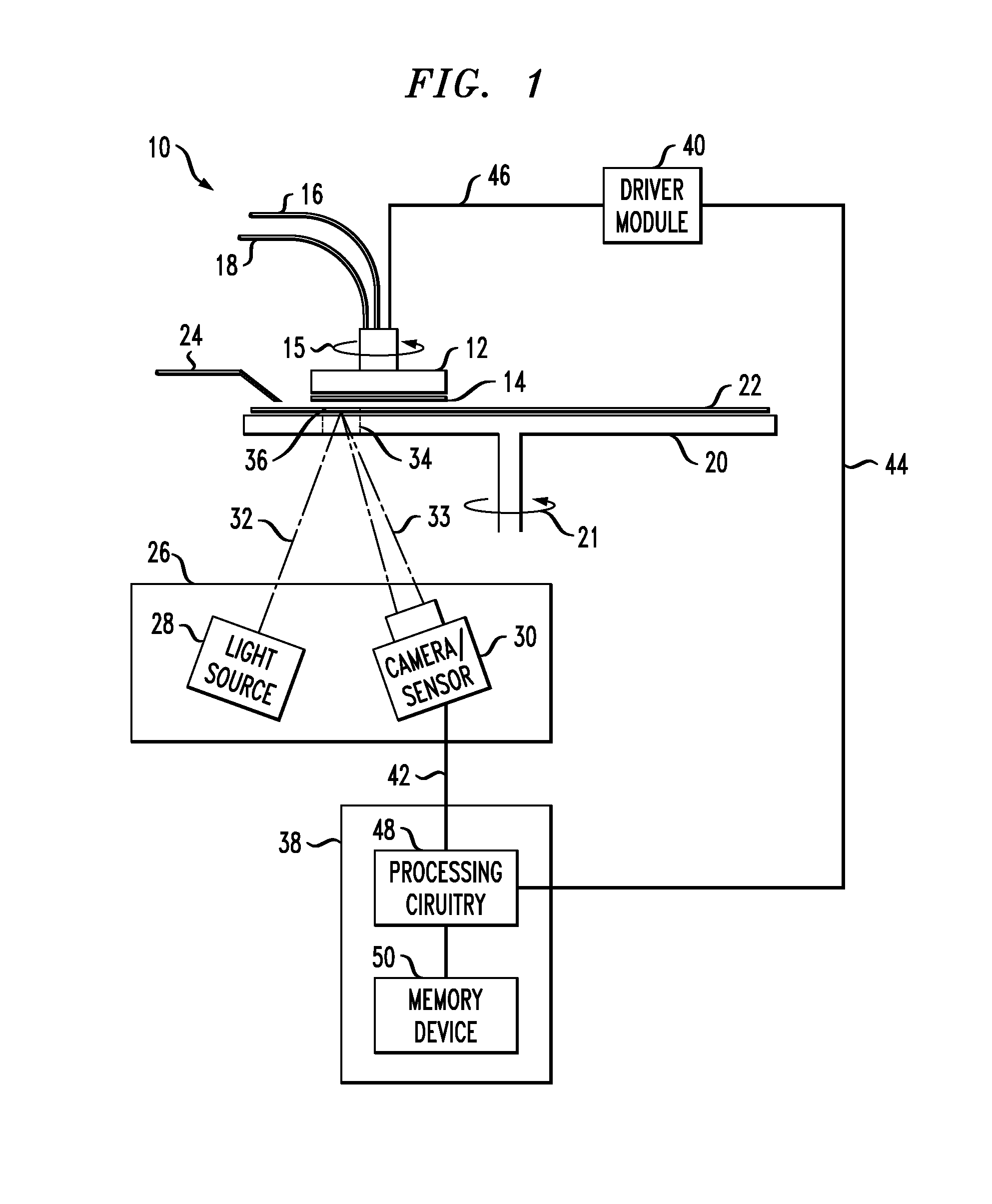
[0028]With reference now to FIG. 1, there is shown a chemical-mechanical polishing (hereinafter “CMP”) tool 10 in accordance with the principles of the present invention. The CMP tool 10 is an electrically active wafer / substrate carrier that is employed to provide adjustment to the thickness of a layer or film of a wafer or layers or films during CMP operations. The CMP tool 10 includes a wafer carrier 12 that is employed to retain a wafer or substrate 14 for CMP operations. The wafer carrier 12 is adapted to be rotated as indicated by the arrow 15, which results in the rotation of the substrate 14. The wafer carrier 12 and thus the substrate 14 is rotating at a high velocity which translates to speeds up to a few hundred linear feet per minute.
[0029]In the CMP tool 10 depicted in FIG. 1, the substrate 14 adheres to the wafer carrier 12 by the use of a vacuum applied to the back of the substrate 14. The wafer carrier 12 includes a wafer carrier vacuum line 16 that provides a vacuum ...
PUM
 Abstract
Description
Claims
Application Information