Method for manufacturing a surface and integrated circuit using variable shaped beam lithography

a beam lithography and integrated circuit technology, applied in the field of lithography, can solve the problems of high cost of computation time, difficult to accurately reproduce the mask pattern and the actual circuit pattern developed on the resist layer, and difficult to add opc features, so as to achieve the effect of reducing the shot coun

Inactive Publication Date: 2010-07-13
D2S
View PDF17 Cites 80 Cited by
  • Summary
  • Abstract
  • Description
  • Claims
  • Application Information

AI Technical Summary

Problems solved by technology

An example of an end-use limitation is defining the geometry of a transistor in a way in which it cannot sufficiently operate at the required supply voltage.
The design rule limitations reflect, among other things, the smallest dimensions that can be reliably fabricated.
As the critical dimensions of the circuit pattern become smaller and approach the resolution value of the exposure tool, the accurate transcription between the mask pattern and the actual circuit pattern developed on the resist layer becomes difficult.
However, as imaging systems are pushed closer to their limits, the ability to produce reticles with sufficiently fine OPC features becomes critical.
Adding OPC features is a very laborious task, requires costly computation time, and results in more expensive reticles.
Not only are OPC patterns complex, but since optical proximity effects are long range compared to minimum line and space dimensions, the correct OPC patterns in a given location depend significantly on what other geometry is in the neighborhood.
There are numerous manufacturing factors that also cause variations, but the OPC component of that overall error is often in the range listed.
As OPC features become more complex, however, the division or fracturing of patterns into a set of non-overlapping simple shapes can result in many billions of simple shapes, resulting in very long reticle write times.

Method used


Image

  • Method for manufacturing a surface and integrated circuit using variable shaped beam lithography
  • Method for manufacturing a surface and integrated circuit using variable shaped beam lithography
  • Method for manufacturing a surface and integrated circuit using variable shaped beam lithography

Examples


Embodiment Construction

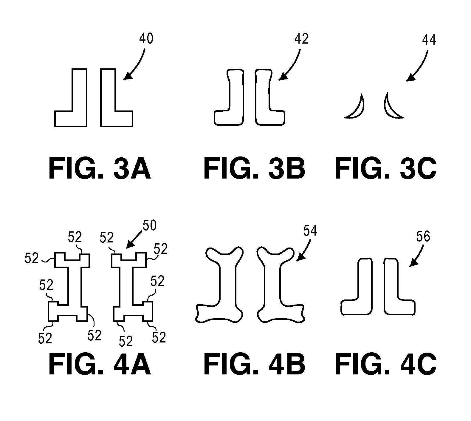
[0060]The improvements and advantages of the present disclosure can be accomplished by allowing overlapping VSB shots and other-than-normal dosages, and by allowing the union of the shots to deviate from the target pattern, allowing patterns to be created from a reduced number of shots compared to the more conventional non-overlapping, normal dosage VSB shots. Thus, a method and a system are provided for manufacturing a surface that addresses the prior problem such as lengthy write time and consequent high cost associated with preparing a surface.

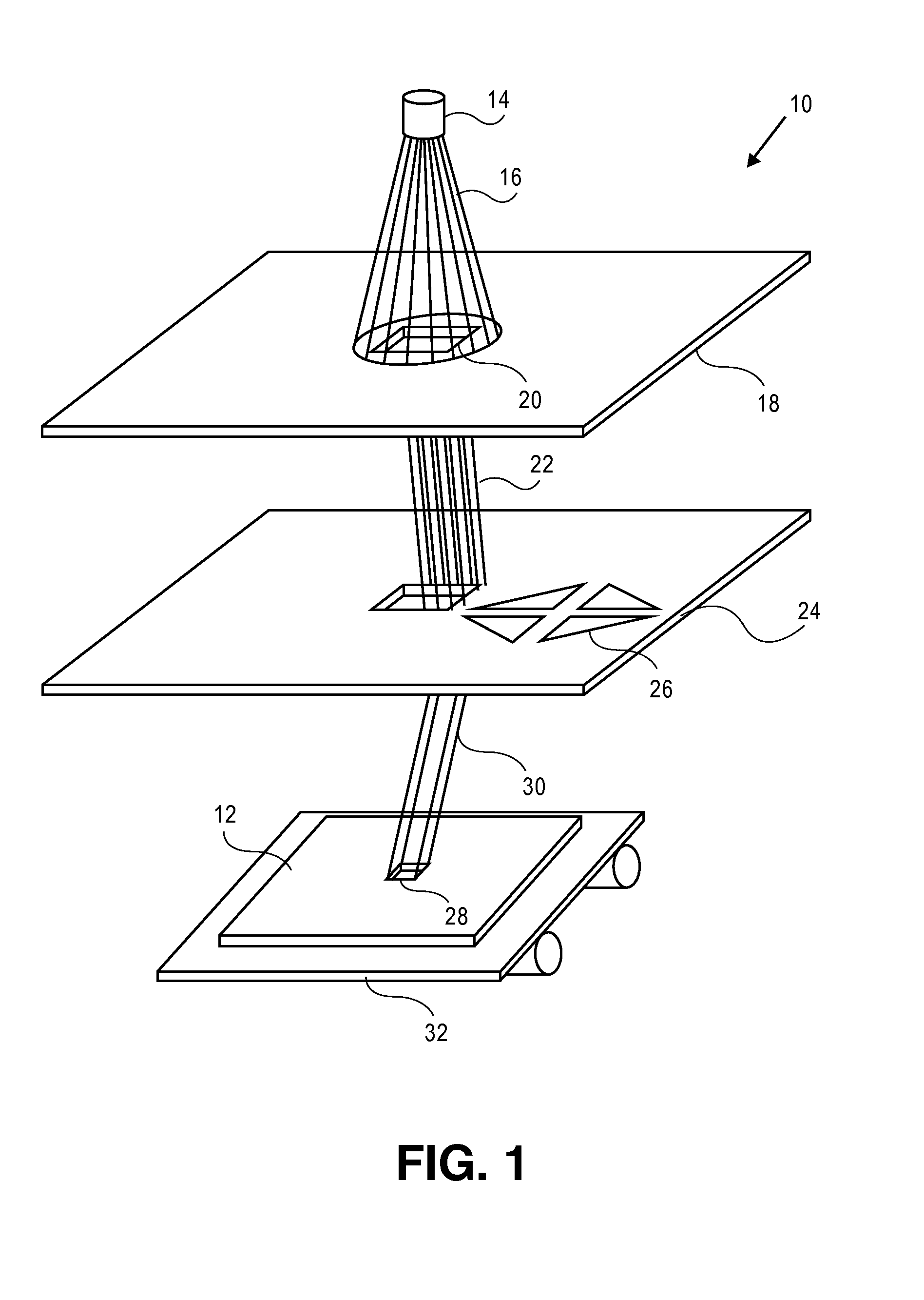
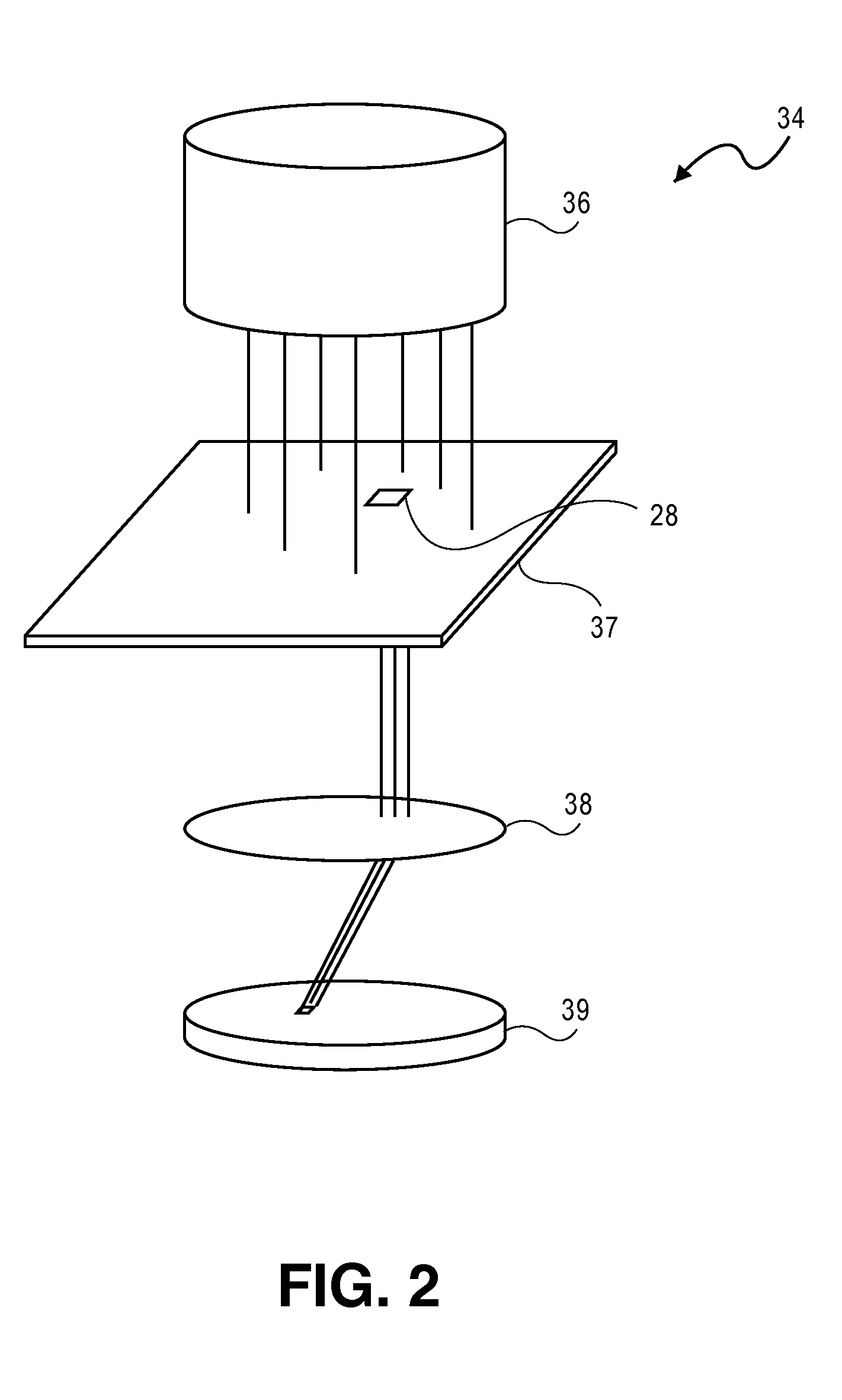
[0061]Referring now to the drawings, wherein like numbers refer to like items, FIG. 1 identifies an embodiment of a lithography system, such as a charged particle beam writer system, in this case an electron beam writer system 10, that employs a variable shaped beam (VSB) to manufacture a surface 12 according to the present disclosure. The electron beam writer system 10 has an electron beam source 14 that projects an electron beam 16 toward...


PUM

PropertyMeasurementUnit
sizeaaaaaaaaaa
aspect ratioaaaaaaaaaa
Optical Proximityaaaaaaaaaa

Abstract

A method is disclosed in which a plurality of variable shaped beam (VSB) shots is used to form a desired pattern on a surface. Shots within the plurality of shots are allowed to overlap each other. Dosages of the shots may also be allowed to vary. The union of the plurality of shots may deviate from the desired pattern. The plurality of shots may be determined such that a pattern on the surface calculated from the plurality of shots is within a predetermined tolerance of the desired pattern. In some embodiments, an optimization technique may be used to minimize shot count. In other embodiments, the plurality of shots may be optionally selected from one or more pre-computed VSB shots or groups of VSB shots. The method of the present disclosure may be used, for example, in the process of manufacturing an integrated circuit by optical lithography using a reticle, or in the process of manufacturing an integrated circuit using direct write.

Description

RELATED APPLICATIONS[0001]This application: 1) is a continuation-in-part of U.S. patent application Ser. No. 12 / 202,364 filed on Sep. 1, 2008 entitled “Method and System for Manufacturing a Reticle Using Character Projection Lithography”; 2) claims priority to U.S. Provisional Patent Application Ser. No. 61 / 172,659, filed on Apr. 24, 2009 and entitled “Method for Manufacturing a Surface and Integrated Circuit Using Variable Shaped Beam Lithography”;3) is related to, U.S. patent application Ser. No. 12 / 473,248, entitled “Method for Optical Proximity Correction of a Reticle to Be Manufactured Using Variable Shaped Beam Lithography,” filed on May 27, 2009; and 4) is related to, U.S. patent application Ser. No. 12 / 473,265, entitled “Method and System for Design of a Reticle to Be Manufactured Using Variable Shaped Beam Lithography,” filed on May 27, 2009; all of which are hereby incorporated by reference for all purposes.BACKGROUND OF THE DISCLOSURE[0002]The present disclosure is relate...

Claims


Application Information

Patent Timeline
Patent Type & Authority Patents(United States)
IPC IPC(8): G03F9/00
CPCB82Y10/00B82Y40/00G03F1/78G03F7/2063H01J37/3174Y10S430/143
Inventor FUJIMURA, AKIRAGLASSER, LANCE
Owner D2S
Why Eureka
Try Eureka