Semiconductor device including capacitor and method of fabricating same

a semiconductor and capacitor technology, applied in semiconductor devices, capacitors, electrical apparatus, etc., can solve the problems of increasing the leakage current in the capacitor, the electrical characteristics of the capacitor are degraded, and the polysilicon layer needs to be formed, so as to improve the leakage current characteristic, and improve the contact resistance.

Inactive Publication Date: 2010-07-20
SAMSUNG ELECTRONICS CO LTD
View PDF14 Cites 0 Cited by
  • Summary
  • Abstract
  • Description
  • Claims
  • Application Information

AI Technical Summary

Benefits of technology

[0013]According to some embodiments of the invention, a semiconductor device has a capacitor with an improved leakage current characteristic and a low level of contact resistance between the capacitor and a metal contact plug. According to other embodiments of the invention, a method of fabricating a semiconductor device having a capacitor with an improved leakage current characteristic and a low level of contact resistance between the capacitor and the metal contact plug may be accomplished at a relatively low temperature.

Problems solved by technology

A disadvantage to the above approach is that a doped polysilicon electrode used as a top / bottom electrode of a conventional capacitor typically reacts with the high-k dielectric layer, degrading the electrical characteristics of the capacitor.
Another disadvantage of using the conventional doped polysilicon electrode is that the doped polysilicon layer needs to be formed at above 600° C. to activate dopants of the polysilicon electrode or a specific thermal treatment is often required.
This high temperature process increases leakage currents in the capacitor.
For MIS capacitors, there may be limitations in integration processes related to wet etching, dry etching, and stress.
Also, since the metal layer has a low resistivity, the metal layer may not be adequate to function as a resistor layer for delaying signals.
Regardless of the capacitor type, in order to decrease the capacitor leakage current while simultaneously achieving highly integrated DRAM cells, it is often necessary to perform processes subsequent to formation of the high-k dielectric layer at a low temperature because the thermal stability of the high-k dielectric layer is not very good.
Also, when an interconnection process is performed after the capacitor formation process, it is often required to decrease a contact resistance level between the top electrode of the capacitor and a metal contact plug.

Method used


Image

  • Semiconductor device including capacitor and method of fabricating same
  • Semiconductor device including capacitor and method of fabricating same
  • Semiconductor device including capacitor and method of fabricating same

Examples


Embodiment Construction

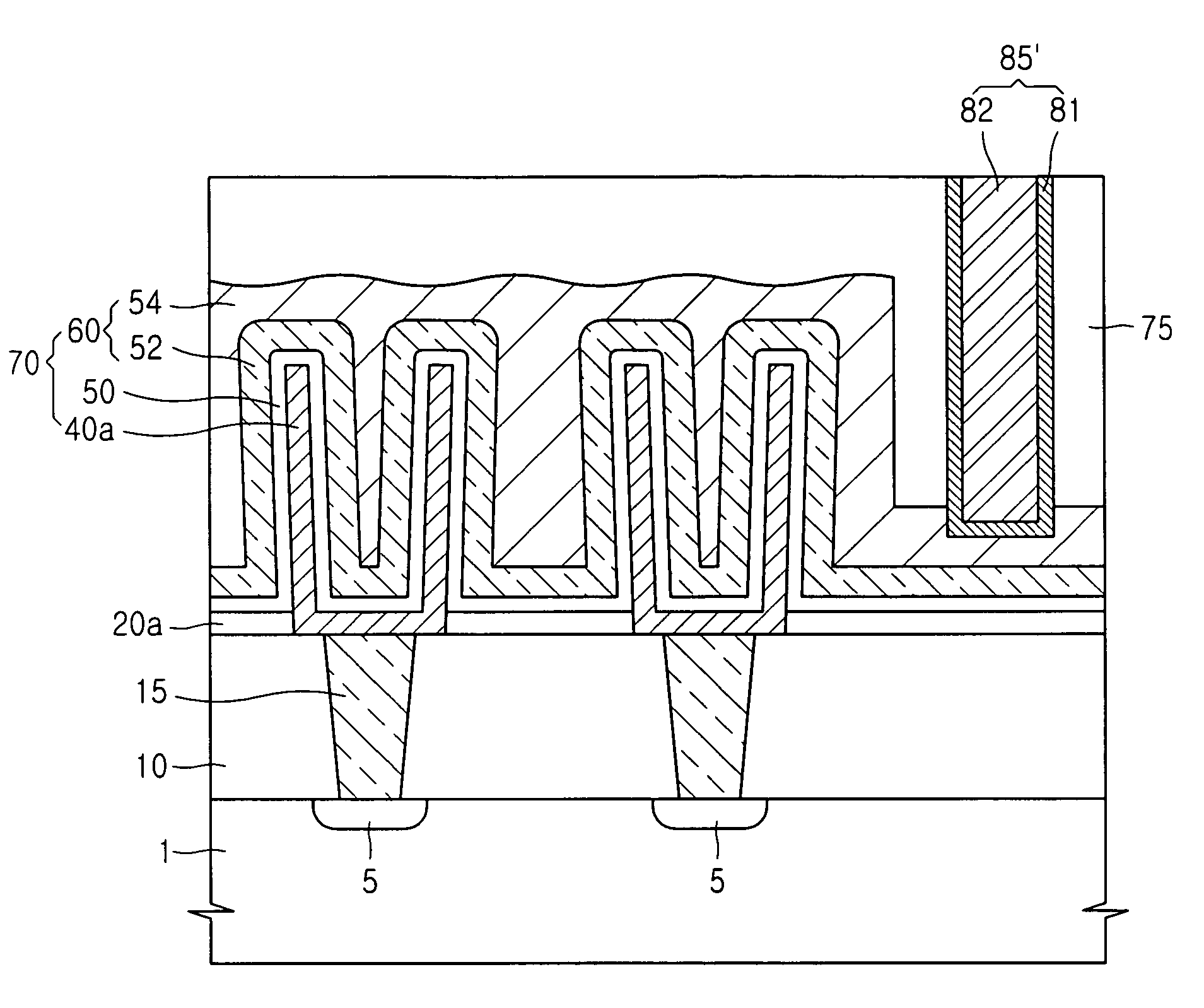
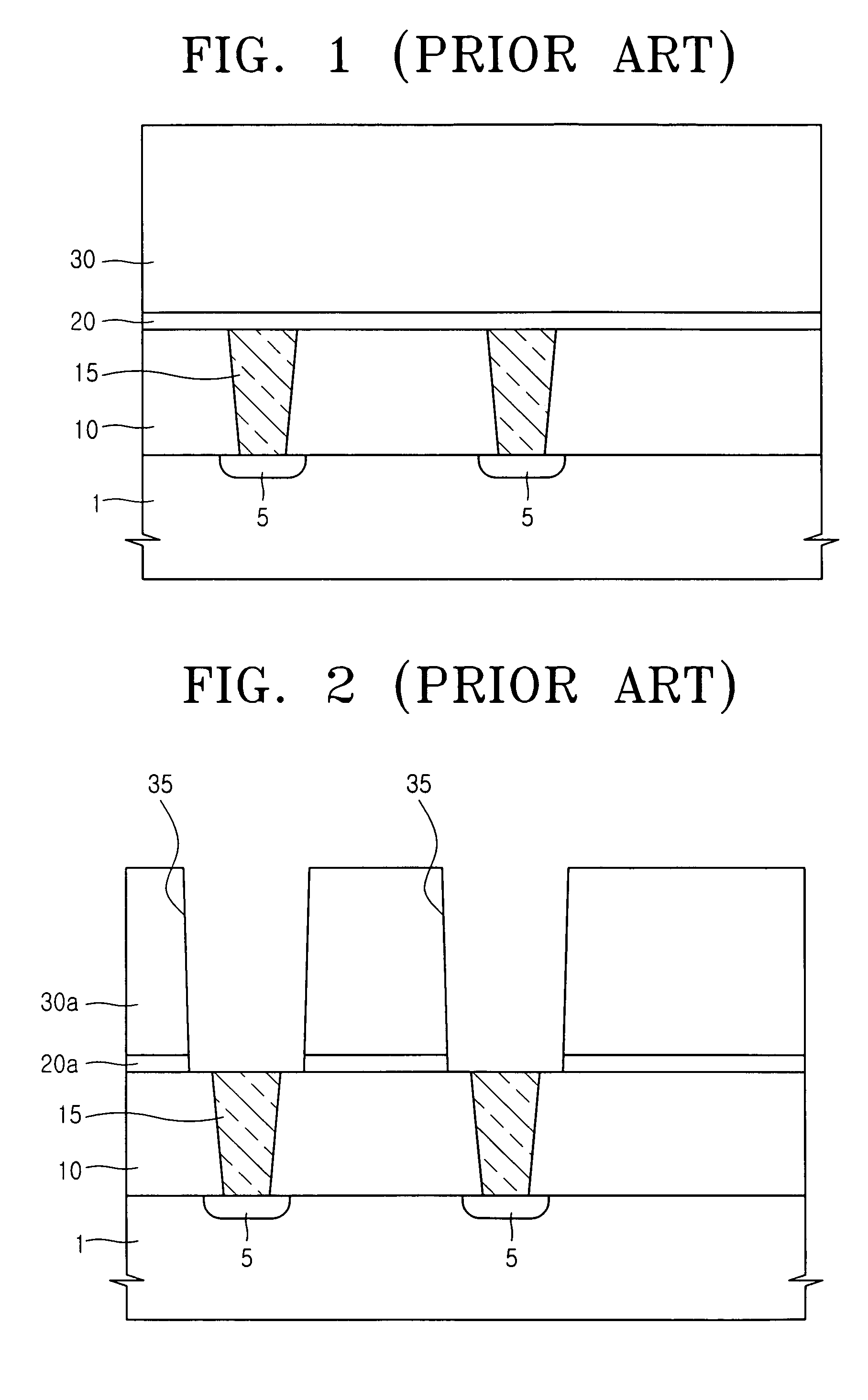
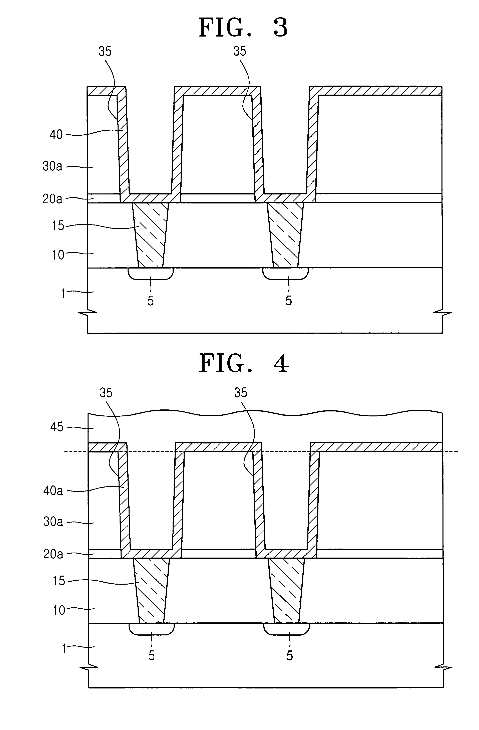
[0023]The invention will be described more fully below with reference to the accompanying drawings in which certain embodiments of the invention are shown. This invention may, however, be embodied in many different forms and should not be construed as being limited to the embodiments set forth herein. Rather, these embodiments are provided so that this disclosure will be thorough and complete, and will fully convey the scope of the invention to those skilled in the art. In the drawings, some features may be exaggerated for clarity. To facilitate understanding, identical reference numerals have been used, where possible, to designate identical elements that are common to the figures.

[0024]FIGS. 1 through 7 are sectional diagrams illustrating a semiconductor device manufactured according to some embodiments of the invention. As will be explained below, the semiconductor device includes a capacitor having a bottom electrode implemented with a doped polysilicon layer and a top electrode...


PUM


Abstract

A semiconductor device includes a capacitor having a bottom electrode, a dielectric layer formed on the bottom electrode, a top electrode formed on the dielectric layer, and a contact plug having a metal that is connected with the top electrode, wherein the top electrode includes a doped poly-Si1-xGex layer and a doped polysilicon layer epitaxially deposited on the doped poly-Si1-xGex layer and the contact plug makes a contact with the doped polysilicon layer.

Description

CROSS-REFERENCE TO RELATED APPLICATIONS[0001]This application claims foreign priority from Korean (KR) Patent Application No. 10-2004-0084867, filed on 22 Oct. 2004. Korean Patent Application No. 10-2004-0084867 is hereby incorporated by reference.BACKGROUND[0002]1. Technical Field[0003]This disclosure relates to semiconductor devices that include capacitors and methods of fabricating the same.[0004]2. Description of the Related Art[0005]As the integration scale of semiconductor devices increases, the cell sizes of semiconductor devices such as Dynamic Random Access Memories (DRAMs) decrease. Consequently, the effective area of a lower electrode in a cell capacitor also decreases. However, a certain level of cell capacitance is generally required for proper device operation.[0006]One approach to achieving a high level of cell capacitance within a limited area is the use of high-k dielectric materials, which have dielectric constants that are several times to several hundreds times h...

Claims


Application Information

Patent Timeline
Patent Type & Authority Patents(United States)
IPC IPC(8): H01L21/8242
CPCH01L28/60H01L28/91H01L21/3142H01L21/31616H01L21/31645H01L27/10814H01L27/10882H01L27/10894H01L21/02181H01L21/02178H10B12/315H10B12/48H10B12/09H10B12/00
Inventor AHN, JAE-YOUNGNOH, JIN-TAEKIM, HEE-SEOKKIM, JIN-GYUNLIM, JU-WANYANG, SANG-RYOLKIM, HONG-SUKLEE, SUNG-HAE
Owner SAMSUNG ELECTRONICS CO LTD
Why Eureka
Try Eureka