

Composite dielectric thin film, capacitor and field effect transistor using the same, and each fabrication method thereof
- Summary
- Abstract
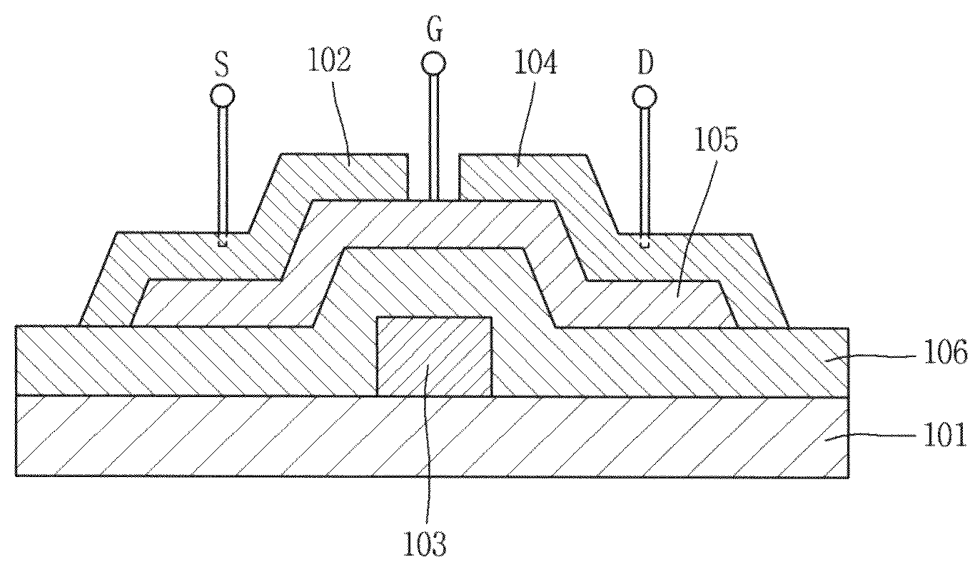
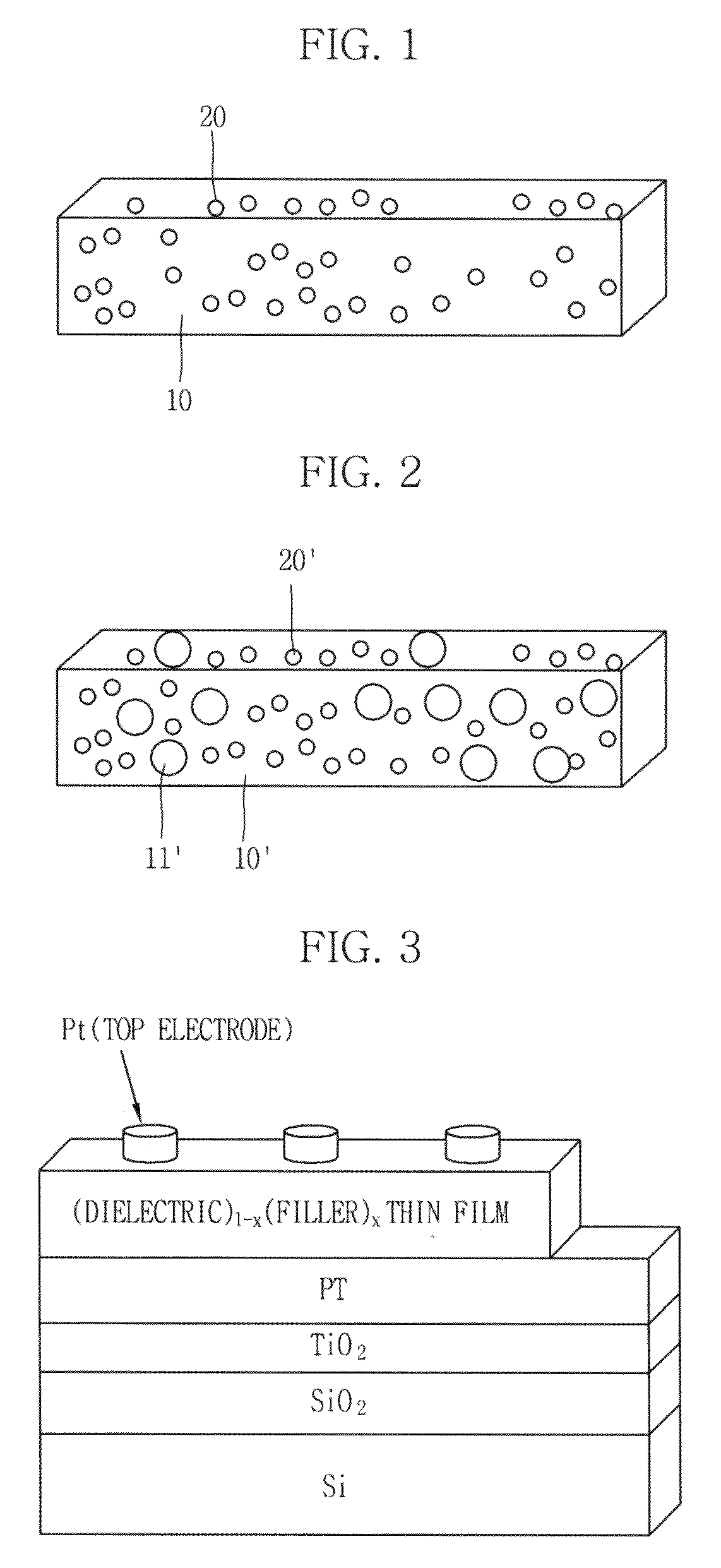
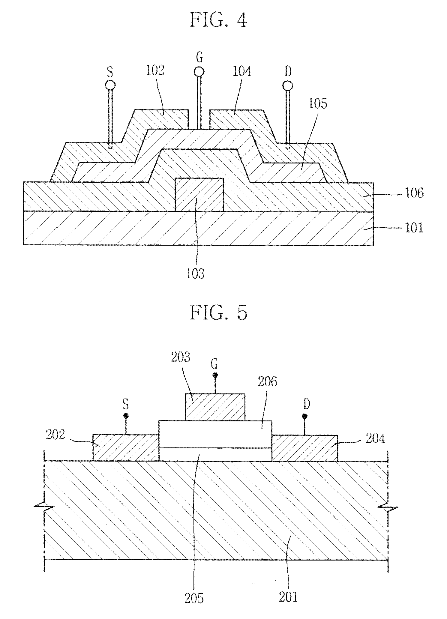
- Description
- Claims
- Application Information
AI Technical Summary
Benefits of technology
Problems solved by technology
Method used
Image

Examples
embodiment 1
(Ba0.6Sr0.4TiO3)1-x—(MgO)x (x=0.1˜0.3) Composite Dielectric Thin Film Using a PLD Method and Fabrication of Capacitor Using the Same
[0068]First, in order to prepare powder having a composition of Ba0.6Sr0.4TiO3, powder of BaCO3, SrCO3, TiO2 was weighted according to a composition ratio of Ba0.6Sr0.4TiO3, and the weighted powder of BaCO3, SrCO3, TiO2 was mixed in an ethanol solvent through ball milling for 24 hours. At this time, zirconia ball was used in performing ball milling. In a Ba0.6Sr0.4TiO3 dielectric, as the ratio of [Ba] and [Sr], other composition ratio than that of 0.6:0.4 used in this embodiment may be used, and there is no restriction to a particular composition ratio. Subsequently, the mixed powder was dried and thermally treated at 1200° C. for three hours to synthesize Ba0.6Sr0.4TiO3 powder.
[0069]Thereafter, 10 mol %, 20 mol %, and 30 mol % of MgO was added to the synthesized Ba0.6Sr0.4TiO3 powder, on which zirconia ball milling was performed for 24 hours, and the r...
embodiment 2
(Ba0.6Sr0.4TiO3)1-x—(MgO)x (x=0.2˜0.3) Composite Dielectric Thin Film Using a Sputtering Method and Fabrication of Capacitor Using the Same
[0075]After Ba0.6Sr0.4TiO3 powder was synthesized in the same manner as in the above-described Embodiment 1, to which 20 mol % and 30 mol % of MgO were added, respectively. Zirconia ball milling was performed on the resultant material for 24 hours, and then, mixing, drying, molding and thermally treating process were performed to obtain a 2-inch ceramic target having a composition of (Ba0.6Sr0.4TiO3)1-x—(MgO)x (x=0.2˜0.3). Finally, the ceramic target was sintered at 1400° C. for five hours to complete the fabrication of a sputtering target.
[0076]Next, a composite dielectric thin film having a thickness of 300 nm was formed at a room temperature by using the obtained target having the composition of (Ba0.6Sr0.4TiO3)1-x—(MgO)x (x=0.2˜0.3). At this time, RF power was 80W, the process pressure was changed from 10 mTorr to 60 mTorr, and Ar and O2, the...
embodiment 3
(Bi1.5Zn1.0Nb1.5O7)1-x—(MgO)x (x=0.1˜0.3) Composite Dielectric Thin Film Using the PLD Method and Fabrication of Capacitor Using the Same
[0083]First, in order to prepare powder having a composition of Bi1.5Zn1.0Nb1.5O7, powder of Bi2O3, ZnO, Nb2O5 was weighted according to a composition ratio of Bi1.5Zn1.0Nb1.5O7, and the weighted Bi2O3, ZnO, Nb2O5 powder was mixed in an ethanol solvent through ball milling for 24 hours. At this time, zirconia ball was used for the ball milling. Subsequently, the mixed powder was dried and thermally treated at 900° C. for three hours to synthesize Bi1.5Zn1.0Nb1.5O7.
[0084]Next, 10 mol %, 20 mol % and 30 mol % of MgO were added to the synthesized Bi1.5Zn1.0Nb1.5O7 powder, respectively, on which zirconia ball milling was performed for 24 hours. The resultant material was mixed, dried, molded and thermally treated to fabricated 1-inch ceramic target having a composition of (Bi1.5Zn1.0Nb1.5O7)1-x—(MgO)x (x=0.1˜0.3). Finally, the ceramic target was sinter...
PUM
| Property | Measurement | Unit |
|---|---|---|
| Temperature | aaaaa | aaaaa |
| Dielectric polarization enthalpy | aaaaa | aaaaa |
| Current | aaaaa | aaaaa |
Abstract
Description
Claims
Application Information