Supercharge Your Innovation With Domain-Expert AI Agents!

Data path circuit in a flash memory device

a flash memory device and data path technology, applied in the direction of digital storage, memory adressing/allocation/relocation, instruments, etc., can solve the problem of unnecessarily consuming power

Inactive Publication Date: 2010-07-20
SK HYNIX INC
View PDF10 Cites 1 Cited by
  • Summary
  • Abstract
  • Description
  • Claims
  • Application Information

AI Technical Summary

Benefits of technology

The present invention relates to a data path circuit in a flash memory device that controls the input and output of data to prevent unnecessary power consumption. The circuit includes a switching means that outputs internal address signals based on a data output control signal. The data output circuit includes a multiplexer that selectively outputs data from different planes and a scramble output multiplexer that divides the data output. The circuit also includes a controller that activates the data output path during a data output interval and cuts off the data input path. Overall, the invention prevents power consumption during data input and output intervals and optimizes the data path circuit's efficiency.

Problems solved by technology

As a result, power is unnecessarily consumed.

Method used


Image

  • Data path circuit in a flash memory device
  • Data path circuit in a flash memory device
  • Data path circuit in a flash memory device

Examples


Embodiment Construction

[0040]Hereinafter, the embodiments of the present invention will be explained in more detail with reference to the accompanying drawings.

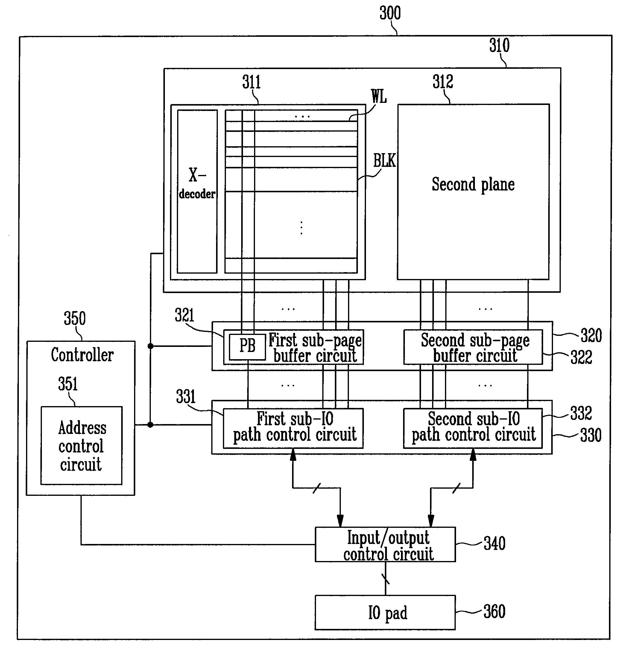
[0041]FIG. 3A is a block diagram illustrating a NAND flash memory device according to one example embodiment of the present invention. The NAND flash memory device 300 includes a plane circuit 310, a page buffer circuit 320, an input / output path control circuit 330, an input / output control circuit 340 and a controller 350.

[0042]The plane circuit 310 includes a first plane 311 and a second plane 312. Each of the planes 311 and 312 includes a memory cell array having memory blocks BLK, wherein each of the memory blocks BLK has memory cells coupled to word lines WL and bit lines BL. In addition, each of the planes 311 and 312 includes an X decoder for selecting the memory block BLK and the word line WL in accordance with an input address.

[0043]The page buffer circuit 320 includes a first sub-page 10 buffer circuit 321 coupled to the first plane 311 an...


PUM


Abstract

A data output circuit in an NAND flash memory device is disclosed. The data path circuit in a flash memory includes at least one switching means configured to output one or more internal address signals in accordance with a data output control signal, and one or more data output circuit configured to output data when a specific internal address signal is outputted through the switching means.

Description

CROSS-REFERENCE TO RELATED APPLICATIONS[0001]This application claims priority from Korean Patent Application No. 2007-41416, filed on Apr. 27, 2007, the contents of which are incorporated herein by reference in its entirety.BACKGROUND OF THE INVENTION[0002]The present invention relates to a data path circuit in a NAND flash memory device. More particularly, the present invention relates to a data path circuit in a NAND flash memory device for reducing power consumed by a data output circuit when data are inputted.[0003]Flash memory is a non-volatile memory for electrically erasing and programming data, and has the advantage of a random access memory RAM where data are freely written and erased and the advantage of a read only memory ROM where data can be maintained without a continuous power source. Hence, the flash memory has been widely used as a storage device for portable electrical devices such as a digital camera, a personal digital assistant PDA, and an MP3 player, etc.[0004]...

Claims


Application Information

Patent Timeline
Patent Type & Authority Patents(United States)
IPC IPC(8): G11C11/34
CPCG11C16/26G06F12/00G06F12/02G06F13/16G06F13/20
Inventor KANG, WON KYUNGKIM, EUI SUK
Owner SK HYNIX INC
Features
  • R&D
  • Intellectual Property
  • Life Sciences
  • Materials
  • Tech Scout
  • Unparalleled Data Quality
  • Higher Quality Content
  • 60% Fewer Hallucinations
Learn More