Light emitting device having high optical output efficiency

a light emitting device and high optical output technology, applied in the field of semiconductor/solid-state device manufacturing, semiconductor devices, electrical apparatus, etc., can solve the problems of difficult to improve optical output efficiency, achieve the effect of suppressing current concentration, preventing electrode material from attaching the sidewall, and improving optical output efficiency

Inactive Publication Date: 2010-07-27
STANLEY ELECTRIC CO LTD
View PDF3 Cites 25 Cited by
  • Summary
  • Abstract
  • Description
  • Claims
  • Application Information

AI Technical Summary

Benefits of technology

[0015]An object of the present invention is to provide a light emitting device capable of improving an optical output efficiency and having a novel structure, and its manufacture method.
[0016]Another object of the present invention is to provide a light emitting device suppressing current concentration upon a region of a semiconductor layer.
[0020]According to the light emitting device of the first aspect, the dent is formed in each section defined by the upper side electrode. Because the dent removes a portion of the optical emission layer that does not contribute to optical emission, but absorbs the emitted light, among other benefits, the optical output efficiency can be improved.
[0021]According to the light emitting device of the second aspect, the first portion of the lower side electrode is formed on the lower semiconductor layer, and the second portion is formed on the support layer having a resistivity higher than that of the lower semiconductor layer. It is therefore possible to suppress concentration of current upon a region near the second portion of the lower side electrode.
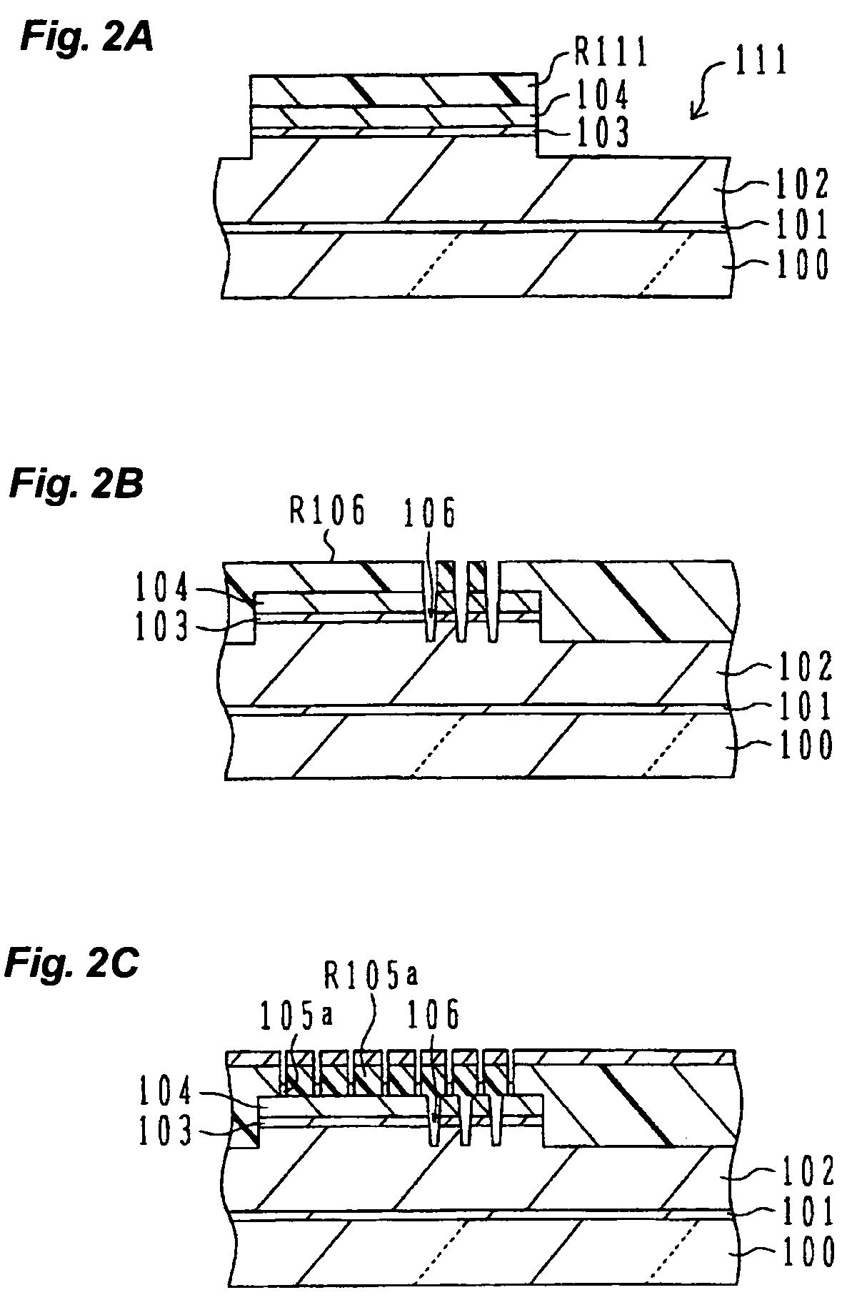
[0022]According to the manufacture method for a light emitting device of the third aspect, the upper side electrode and lower side electrode are formed after the dents are formed. It is therefore possible to prevent electrode material from attaching the sidewalls of the dents during a dent forming process.

Problems solved by technology

It is therefore difficult to improve an optical output efficiency.

Method used


Image

  • Light emitting device having high optical output efficiency
  • Light emitting device having high optical output efficiency
  • Light emitting device having high optical output efficiency

Examples


first embodiment

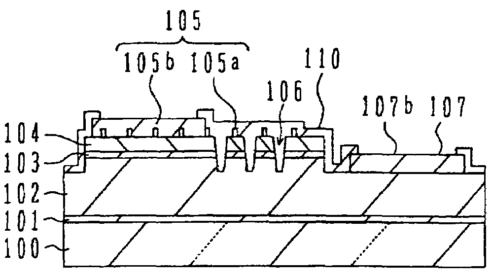
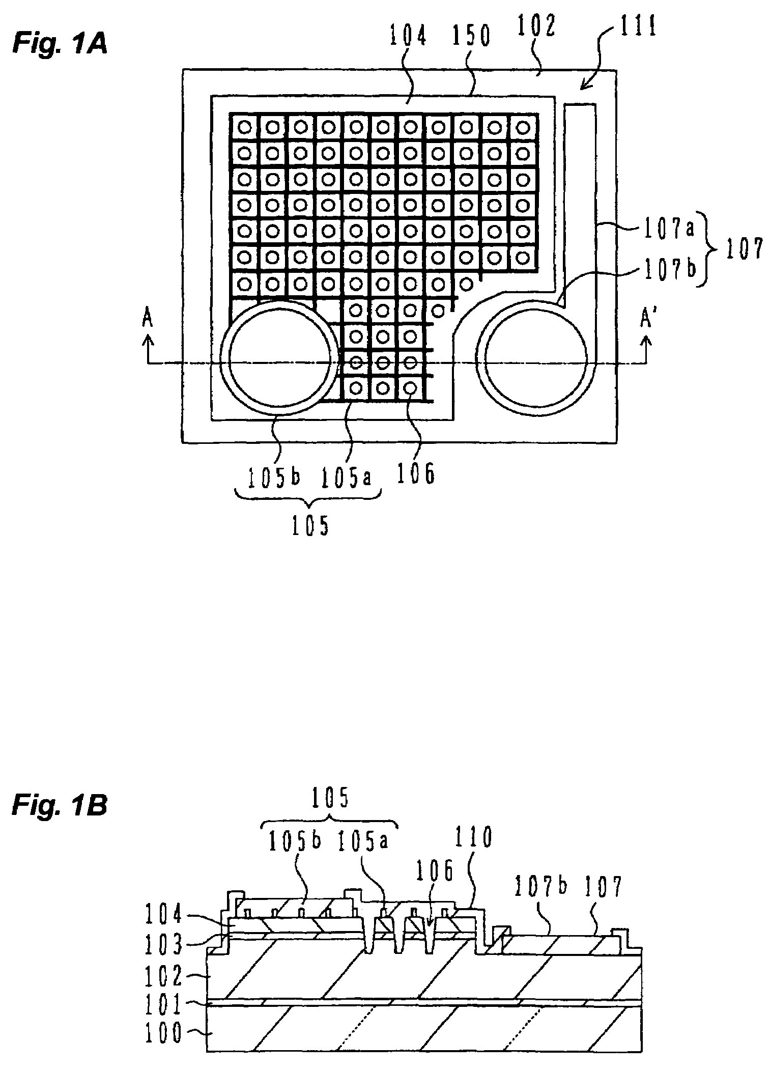
[0056]Next, with reference to FIGS. 1A and 1B, description will be made on a light emitting device according to the present invention.

[0057]FIG. 1A is a schematic plan view of the light emitting device according to the first embodiment, and FIG. 1B is a schematic cross sectional view of the light emitting device of the first embodiment taken along the line A-A′ shown in FIG. 1A.

[0058]The nitride semiconductor wafer described with reference to FIG. 19 is used as the material of the light emitting device of this embodiment. An optical emission region 150 is defined on the surface of a p-type nitride semiconductor layer 104, the optical emission region 150 having a square shape with a recess at one corner. The p-type nitride semiconductor layer 104, an optical emission layer 103 and a surface layer of an n-type nitride semiconductor layer 102, in an area surrounding the optical emission area 150, are removed to form a recess 111 (contour groove 111) exposing the n-type nitride semicond...

second embodiment

[0173]Next, with reference to FIG. 9B, the operation and effects of the lattice portion 205a of the light emitting device of the second embodiment will be described.

[0174]Consider light emitted from the region of the optical emission layer 103 disposed under the coupling part of the lattice portion 205a. Consider that this region is divided into sub-regions along the longitudinal direction of the coupling part. Light emitted from each divided sub-region along the longitudinal direction of the coupling part is accumulated. It can therefore be considered that light emitted along the longitudinal direction of the coupling part becomes stronger than the light emitted along other directions. Light emitted from the region disposed under the linear portion of the p-side electrode along the longitudinal direction of the linear portion is referred to as “electrode parallel propagating light.”

[0175]The dent 206 disposed in the square part connecting the above-described coupling parts is posit...

third embodiment

[0196]There is a tendency that a region of the optical emission layer having a high current density is degraded. In the light emitting device of the third embodiment, current in the optical emission layer can be dispersed so that degradation of the light emitting device can be suppressed.

[0197]Next, with reference to FIGS. 12A to 12C, a light emitting device of a fourth embodiment will be described. FIG. 12A is a schematic plan view of the light emitting device of the fourth embodiment, and FIGS. 12B and 12C are schematic cross sectional views respectively taken along the lines A-A′ and B-B′ shown in FIG. 12A.

[0198]The light emitting device of this embodiment uses a nitride semiconductor wafer similar to that used by the light emitting devices of the first and second embodiments and comparative example.

[0199]In the light emitting device of this embodiment, a region 413 (n-side pad layout region 413) of a contour groove 411 where a pad portion 407b of the n-side electrode 407 is disp...


PUM


Abstract

A light emitting device includes a lower semiconductor layer of a first conductivity type; an optical emission layer formed on said lower semiconductor layer; an upper semiconductor layer of a second conductivity type opposite to said first conductivity type, said upper semiconductor layer being formed on said optical emission layer; a lower side electrode electrically connected to said lower semiconductor layer; and an upper side electrode electrically connected to said upper semiconductor layer, wherein said upper side electrode is formed on said upper semiconductor layer, and said upper semiconductor layer has a mesh pattern defining a plurality of sections each surrounded by said upper side electrode, and wherein at least one dent is disposed in at least one of said sections, said dent having a bottom reaching at least an upper surface of said lower semiconductor layer and having an opening with an upper edge spaced apart from said upper side electrode.

Description

CROSS REFERENCE TO RELATED APPLICATION[0001]This application is based on and claims priority of Japanese Patent Application No. 2005-317308 filed on Oct. 31, 2005, the entire contents of which are incorporated herein by reference.BACKGROUND OF THE INVENTION[0002]A) Field of the Invention[0003]The present invention relates to a semiconductor light emitting device and its manufacture method.[0004]B) Description of the Related Art[0005]With reference to FIG. 22, description will be made on a light emitting device disclosed in U.S. Pat. No. 6,885,034. A semiconductor layer 1028 is formed on a substrate 1014, with a low resistance semiconductor layer 1018 being interposed therebetween. An electrode is connected to the semiconductor layer 1018. A reflection layer 1015 is formed on the bottom surface of the substrate 1014. An optical emission layer 1026 is formed on the semiconductor layer 1028, and a semiconductor layer 1027 is formed on the optical emission layer 1026. The semiconductor ...

Claims


Application Information

Patent Timeline
Patent Type & Authority Patents(United States)
IPC IPC(8): H01L27/15H01L33/00H01L31/12H01L29/18H01L33/06H01L33/14H01L33/24H01L33/32H01L33/38H01L33/40H01L33/44
CPCH01L33/08H01L33/20H01L33/38H01L2933/0016H01L2924/0002H01L2924/00
Inventor TANAKA, SATOSHIHORIO, NAOCHIKATSUCHIYA, MASAHIKO
Owner STANLEY ELECTRIC CO LTD
Why Eureka
Try Eureka