Optical recording medium, and, method for manufacturing the same, and method and apparatus for optical recording and reproducing thereof
a technology of optical recording medium and optical recording medium, which is applied in the field can solve the problems of not being able to meet the requirements of optical recording medium having two recording dye layers, not being able to meet the requirements of optical recording medium, not being able to achieve the effect of reducing the frequency of trouble occurrence, and excellent jitter properties for recording and reproducing
- Summary
- Abstract
- Description
- Claims
- Application Information
AI Technical Summary
Benefits of technology
Problems solved by technology
Method used
Image
Examples
example 1
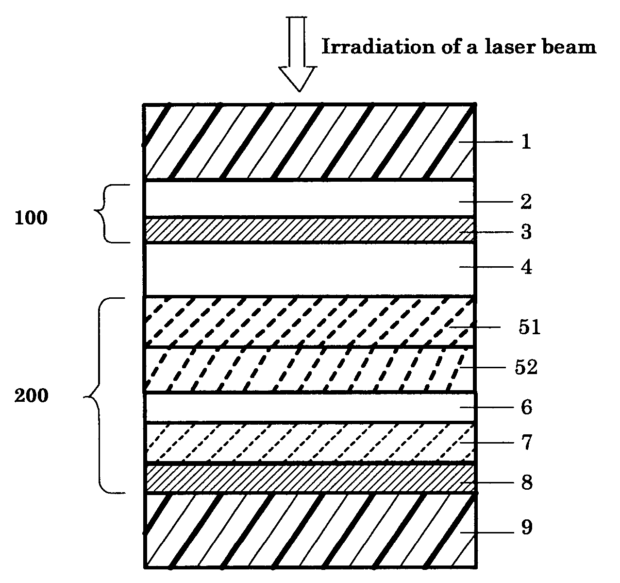
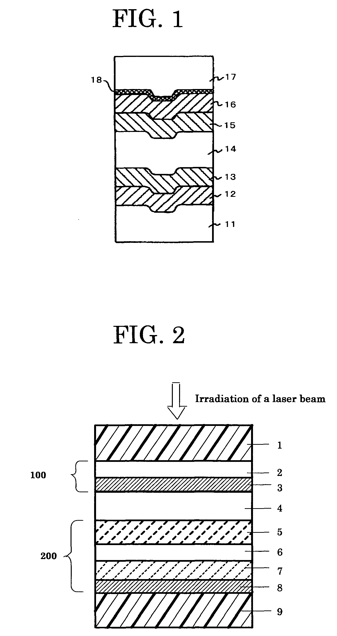
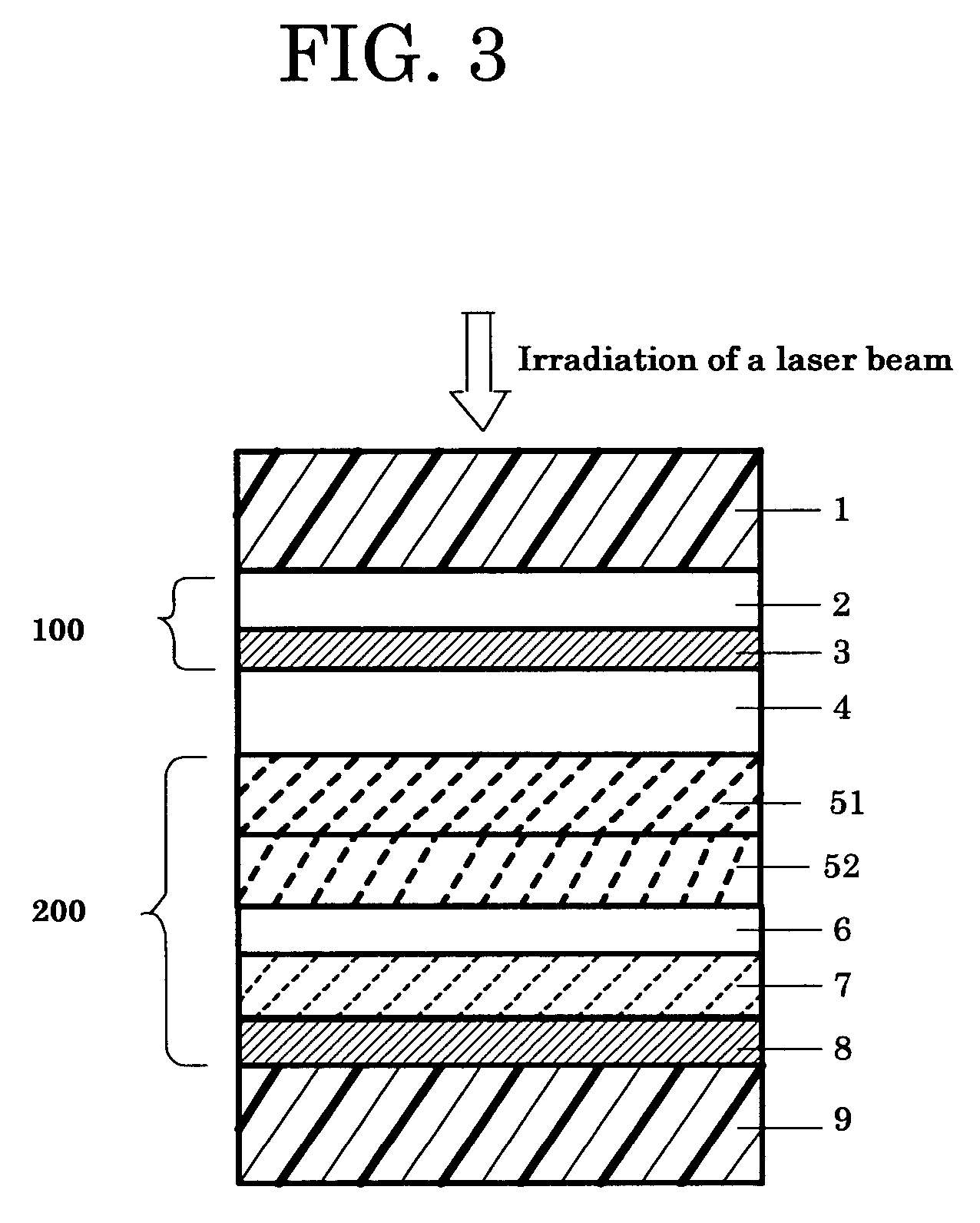
[0094]A substrate made from a polycarbonate resin having a diameter of 12 cm and a thickness of 0.57 mm with concaves and convexes consecutively formed thereon for a tracking guide was prepared.
[0095]First, a squarylium dye expressed by the following formula was dissolved in a tetrafluoropropanole to prepare a coating solution. The coating solution was coated on the substrate by spin-coating to form a first dye layer having a thickness of 100 nm and then the first dye layer was dried at 100° C. for 30 minutes.
[0096]
[0097]Next, a semi-translucent reflective layer made from Ag98In2 was formed on the first dye layer so that the semi-translucent reflective layer had a thickness of 12 nm by sputtering.
[0098]With the above noted processes, a first information layer was formed on the substrate.
[0099]Then, a cover substrate made from a polycarbonate resin having a diameter of 12 cm and a thickness of 0.6 mm was prepared.
[0100]A reflective layer made from Ag98In2 was formed on the cover subs...
examples 2 thorough 16
and Comparative Examples 1 Through to 3
[0108]Individual optical recording media for Examples 2 through 16 and Comparative Examples 1 through 3 were prepared in the same manner as Example 1 except that individual layers thereof were formed by using the materials shown in Table 1, with the respective thicknesses shown in Table 2. It should be noted that in Comparative Example 1 to 3 no oxidized layer was provided; in Examples 14 to 16 a reflectance-reduced layer made from MgF, SiO2, and a fluorocarbon resin, was formed on the surface of the substrate; in Examples 4 to 16 and Comparative Example 2 a protective layer was structured into two layers; and in Examples 2 through 16 and Comparative Example 3, a heat resistant layer was formed and provided.
[0109]
TABLE 1Semi-Protectivetranslucent1st pro-layer or2ndHeat1st dyereflectiveIntermediatetective2nd protec-dyeOxidationReflectiveresistantCoverSubstratelayerlayerlayerlayertive layerlayerlayerlayerlayersubstrateEx. 1Poly-SquaryliumAg98In2U...
PUM
| Property | Measurement | Unit |
|---|---|---|
| thickness | aaaaa | aaaaa |
| thickness | aaaaa | aaaaa |
| thickness | aaaaa | aaaaa |
Abstract
Description
Claims
Application Information


