Formation of SOI by oxidation of silicon with engineered porosity gradient

a technology of porosity gradient and silicon, applied in the direction of semiconductor devices, semiconductor/solid-state device details, electrical apparatus, etc., can solve the problems of unfavorable soi structure formation

Inactive Publication Date: 2010-08-10
GLOBALFOUNDRIES INC
View PDF9 Cites 151 Cited by
  • Summary
  • Abstract
  • Description
  • Claims
  • Application Information

AI Technical Summary

Problems solved by technology

However, forming SOI structures is no simple matter.
While producing SOI wafers of excellent quality, both of these processes are still relatively costly.
The need for pre-patterning made the FIPOS method unwieldy and expensive.
However the process proposed in Choe et al. can not provide tight control over the BOX layer and SOI thicknesses.
Furthermore, the gradual variation in porosity within the buried porous silicon layer makes it difficult to form a BOX layer that has a thickness of less than 100 nanometers (nm).
Forming SOI wafers having a plurality of internal buried oxide layers is also expensive and difficult by bond and etchback or bond and layer transfer methods, because the methods have to be applied at least twice during processing.
To do so by an implantation of oxygen method can also be extremely difficult or even impossible because of the difficulty in controlling the depth of implanted ions to within a relatively narrow range of depths for forming each buried oxide layer.

Method used


Image

  • Formation of SOI by oxidation of silicon with engineered porosity gradient
  • Formation of SOI by oxidation of silicon with engineered porosity gradient
  • Formation of SOI by oxidation of silicon with engineered porosity gradient

Examples


Embodiment Construction

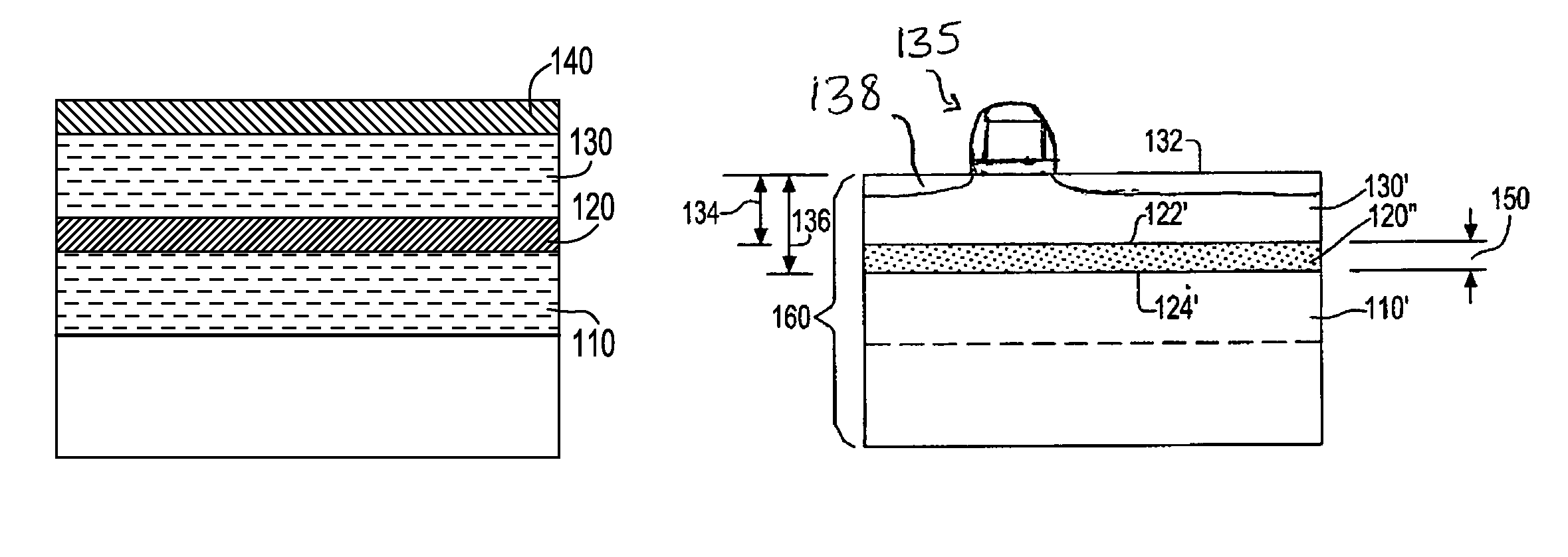
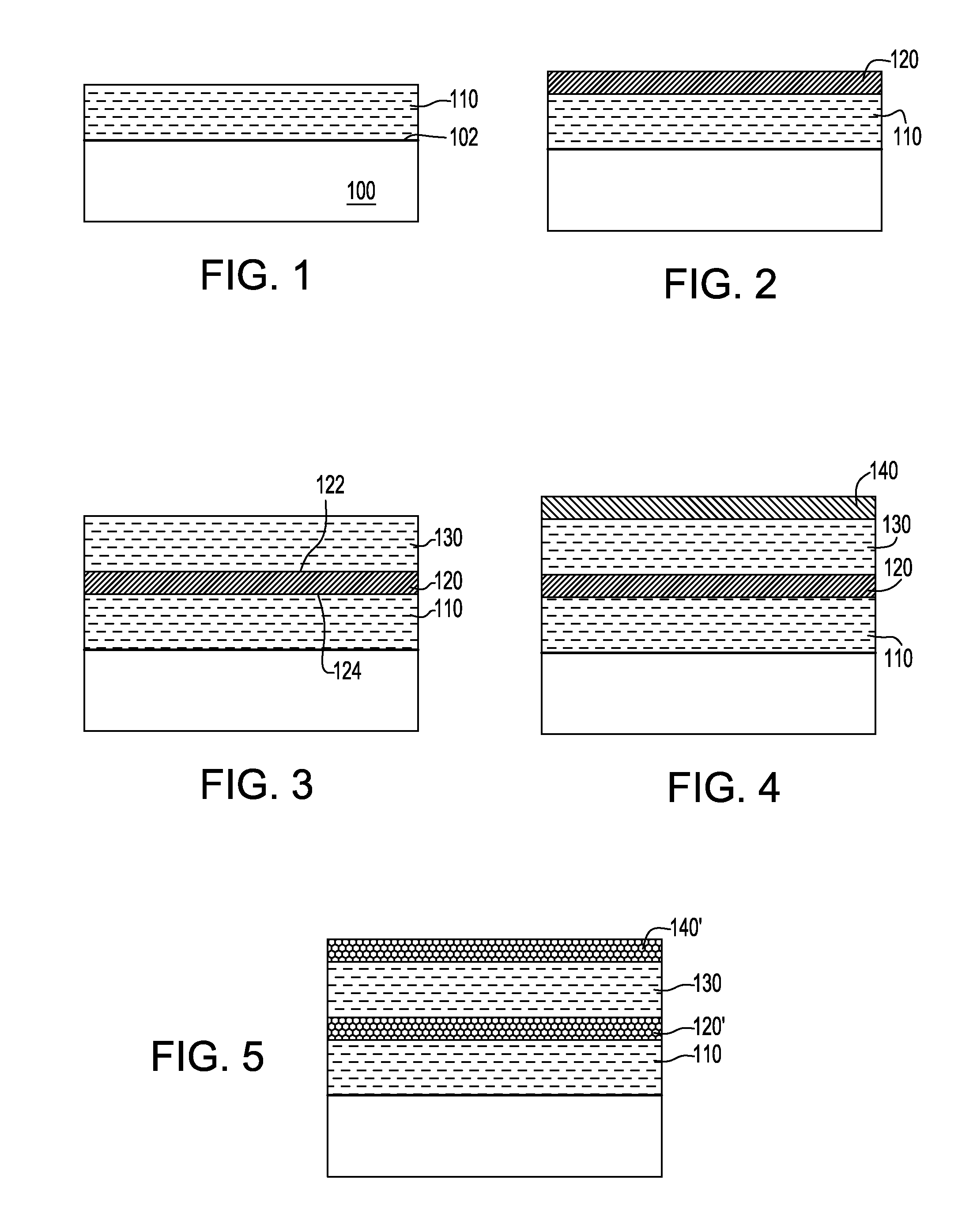
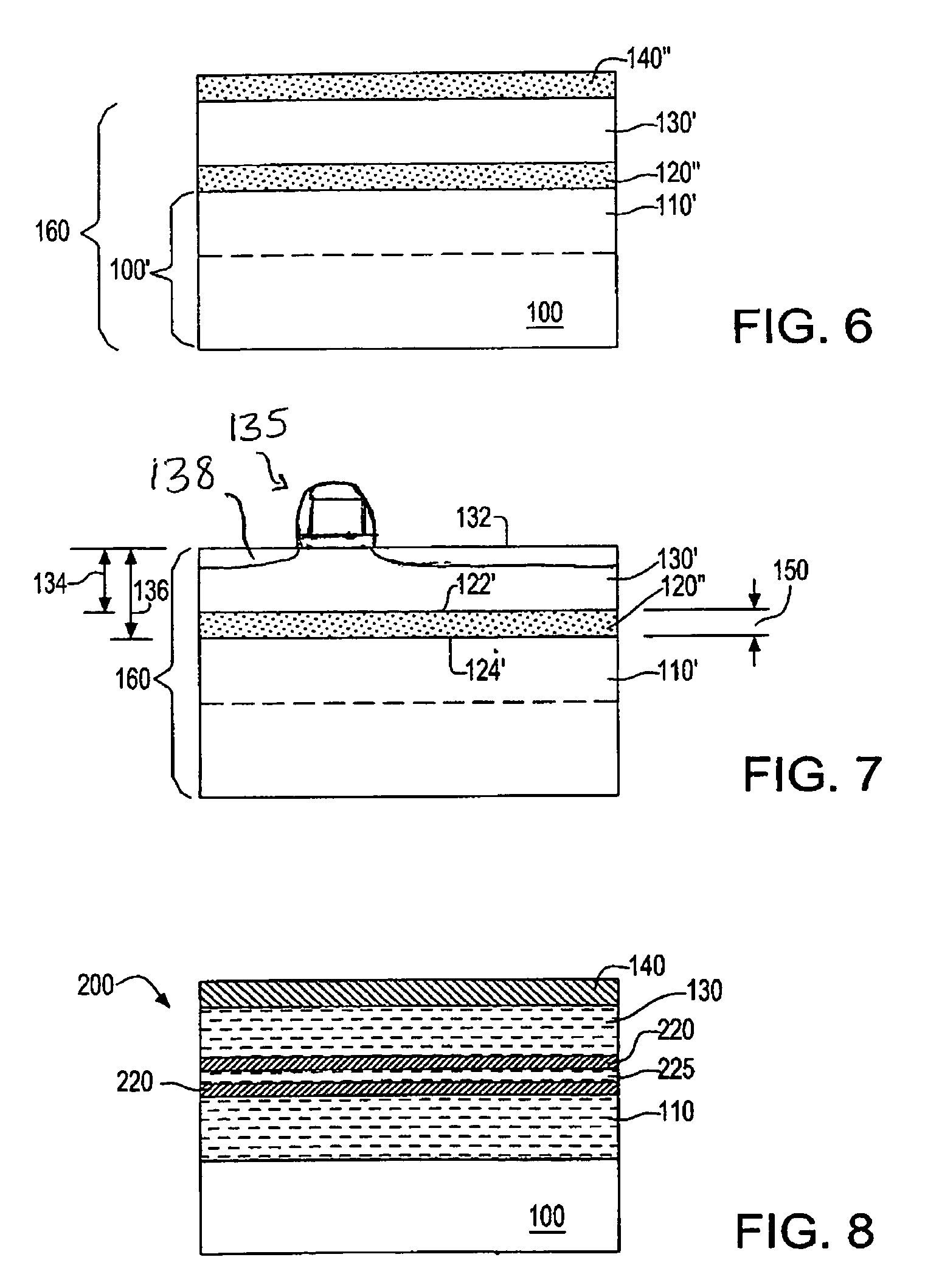
[0021]A feature of a method of fabrication described in accordance with an embodiment of the invention illustrated in FIGS. 1-6 is epitaxial growth of a series of monocrystalline semiconductor layers having differing p-type dopant concentrations which can be established by an in situ doping method. Unlike the ion implantation process described above in Choe et al. as background herein, an in situ doping method establishes a dopant concentration in a semiconductor layer by controlling a concentration of a dopant material present in a chamber while epitaxially growing the semiconductor layer. The epitaxial layer growth method permits creation of layers each having uniform dopant concentration with sharp transition to the adjacent layers of different dopant concentrations. Thus, in an embodiment of the invention herein, a series of vertically stacked epitaxial semiconductor layers can be doped to different p-type dopant concentrations by controlling concentrations of dopant material pr...


PUM

PropertyMeasurementUnit
distanceaaaaaaaaaa
thicknessaaaaaaaaaa
thicknessaaaaaaaaaa

Abstract

A method is provided for making a silicon-on-insulator substrate. Such method can include epitaxially growing a highly p-type doped silicon-containing layer onto a major surface of an underlying semiconductor region of a substrate. Subsequently, a non-highly p-type doped silicon-containing layer may be epitaxially grown onto a major surface of the p-type highly-doped epitaxial layer to cover the highly p-type doped epitaxial layer. The overlying non-highly p-type doped epitaxial layer can have a dopant concentration substantially lower than the dopant concentration of the highly p-type doped epitaxial layer. The substrate can then be processed to form a buried oxide layer selectively by oxidizing at least portions of the highly p-type doped epitaxial layer covered by the non-highly p-type doped epitaxial layer, the buried oxide layer separating the overlying monocrystalline semiconductor layer from the underlying semiconductor region. Such processing can be performed while simultaneously annealing the non-highly p-type doped epitaxial layer.

Description

BACKGROUND OF THE INVENTION[0001]1. Technical Field[0002]The present invention relates generally to semiconductor devices, and more particularly to a silicon-on-insulator substrate and a method for fabricating a silicon-on-insulator substrate.[0003]2. Description of the Related Art[0004]Silicon-on-insulator (“SOI”) wafers are a basic material for use in the fabrication of advanced complementary metal oxide semiconductor (“CMOS”) circuits. An SOI wafer typically includes a relatively thin monocrystalline layer of silicon exposed at an external major surface of the wafer, a bulk semiconductor region typically consisting essentially of silicon underlying the monocrystalline silicon layer, and a buried oxide (BOX) layer separating the monocrystalline layer from the bulk semiconductor region. The buried oxide layer typically has a thickness of less or about 150 nanometers (nm) and consists essentially of amorphous silicon dioxide.[0005]The separation or isolation of the overlying monocry...

Claims


Application Information

Patent Timeline
Patent Type & Authority Patents(United States)
IPC IPC(8): H01L21/20H01L21/36
CPCH01L21/76245
Inventor DESOUZA, JOEL P.FOGEL, KEITH E.REZNICEK, ALEXANDERSADANA, DEVENDRA
Owner GLOBALFOUNDRIES INC
Why Eureka
Try Eureka