Level shifter circuit to shift signals from a logic voltage to an input/output voltage
Active Publication Date: 2010-08-10
NVIDIA CORP
3 Cites 2 Cited by
AI-Extracted Technical Summary
Problems solved by technology
As the difference in voltage levels between the I/O circuitry and logic circuitry increases, the difficulty of shifting the voltage level of signals from the logic domain to the I/O domain is increased.
However, when a silicon process is used that allows the size of logic circuitry to be reduced to use a VDD_Logic of 0.9 volts, such as a 45 nanometer process, circuit 100 may not functi...
Benefits of technology
[0014]One advantage of the disclosed voltage level shifting circuit is that it uses a combination of I/O and logic transistors to avoid exceeding a maximum tolerable voltage across the gate and source of any of the transistors. Therefore, the voltage level shifting circuit is not sensitive to scaling of the low voltage supply and operates properly when the low voltage supply is reduced due ...
Abstract
One embodiment of the present invention sets forth a technique for shifting the voltage level of signals from the high voltage domain to a low voltage domain, where VDD_IO is the supply voltage of the high voltage domain and VDD_Logic is the supply voltage of the low voltage domain. A level shifting circuit using a combination of I/O and logic transistors avoids exceeding a maximum tolerable voltage across the gate and source of any of the transistors. The level shifting circuit operates includes a reference voltage circuit that is independent of VDD_IO, so the same level shifting circuit may be used for various VDD_IO voltages. Additionally, the voltage level shifting circuit is not sensitive to scaling of VDD_Logic and operates properly when VDD_Logic is reduced due to shrinking silicon process technology and/or is reduced for a low power application.
Application Domain
Pulse automatic controlElectric pulse generator +1
Technology Topic
Voltage referenceInput/output +6
Image
Examples
- Experimental program(1)
Example
[0027]In the following description, numerous specific details are set forth to provide a more thorough understanding of the present invention. However, it will be apparent to one of skill in the art that the present invention may be practiced without one or more of these specific details. In other instances, well-known features have not been described in order to avoid obscuring the present invention.
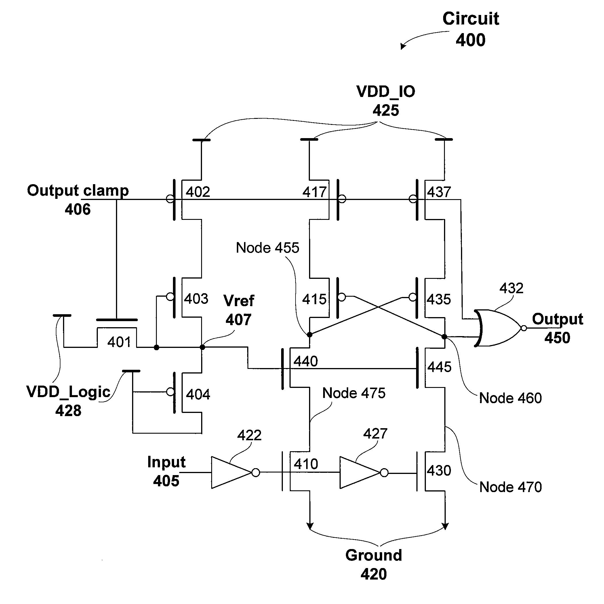
[0028]FIG. 3 is a block diagram illustrating a device 300 that includes a voltage level shifter 320 configured to implement one or more aspects of the present invention. Logic circuits 330 is within a low voltage domain 324 and operates at a VDD_logic voltage level that is lower than the VDD_IO voltage level used by I/O circuits 315. I/O circuits 315 is within a high voltage domain 322 and may include pads and other I/O specific circuits that operate at the VDD_IO voltage to send and receive signals from other devices in a system that also operate at the VDD_IO voltage. Output signals 301 through 305 are produced by I/O circuits 315 based on signals received by voltage level shifters 320 and 325 from the low voltage domain 324.
[0029]Voltage level shifters 320 and 325 are within both the high voltage domain 322 and the low voltage domain 324 and shift the signals from the VDD_Logic voltage used in the low voltage domain 324 to the VDD_IO voltage level used in the high voltage domain 322 to produce output signals 301 through 305. Voltage level shifters are described in detail in conjunction with FIGS. 4B, 4C, 4D, 4E, 5A, and 5B. Although voltage level shifters 320 and 325 are shown in FIG. 3 as shifting signals from the low voltage domain 324 to the high voltage domain 322, the voltage level shifters 320 and 325 may also be used to shift signals from any circuitry operating at a voltage that is lower than the VDD_IO voltage to the high voltage domain 322. In other words, the voltage level shifters 320 and 325 are configured to shift signals from a low voltage domain to a high voltage domain, where the high voltage domain operates using a voltage supply that is at a higher voltage compared with the voltage supply used by devices in the low voltage domain.
[0030]FIG. 4A illustrates a voltage reference circuit 412 that is independent of the high voltage domain supply, VDD_IO 425, according to one embodiment of the invention. Transistors 401, 404, 403, and 402 are all input/output devices that are designed to operate at VDD_IO 425. Output clamp 406 is the output clamp input. Voltage reference circuit 412 is configured in an operation mode when ground is applied to output clamp 406 and voltage reference circuit 412 is configured in a clamp mode when VDD_IO is applied to output claim 406. When voltage reference circuit 412 is in operation mode, transistor 402 is activated and transistor 404 is activated when Vref 407 is greater than or equal to the sum of VDD_Logic 428 and the threshold voltage of the input/output transistors, Vth_IO. Transistor 403 is activated when Vref 407 is less than or equal to the difference between VDD_IO 425 and Vth_IO. Therefore, Vref 407 ranges in value between VDD_Logic+Vth_IO and VDD_IO−Vth_IO.
[0031]Transistors 404 and 403 may be sized such that the width of transistor 403 is less than the width of transistor 404, resulting in transistor 404 having a smaller resistance compared with transistor 403 and Vref 407 that approximately equals VDD_Logic+Vth_IO when voltage reference circuit 412 is configured in the operation mode. When voltage reference circuit 412 is configured in the clamp mode, Vref 407 equals VDD_Logic. Importantly, Vref 407 is independent of the high voltage domain supply, VDD_IO 425, and operates as the logic circuitry size changes.
[0032]FIG. 4B illustrates a level shifter circuit 400 for shifting signals from a low voltage domain to high voltage domain, according to one embodiment of the invention. Input signal 405 is level shifted from a VDD_Logic voltage to a VDD_IO voltage, producing an output signal 450. Unlike circuits 100 and 200, voltage level shifter circuit 400 is not sensitive to VDD_Logic scaling or transistor failure due to gate oxide reliability. Level shifter circuit 400 functions properly using Vref 407 that is independent of VDD_IO 425. Transistors 401, 402, 403, and 404 are configured to form the voltage reference circuit 412. Inverters 422 and 427 and transistors 410 and 430 are the only logic devices in level shifter circuit 400. The gates of PMOS I/O transistors 402, 417, and 437 and a first input to a NOR gate 432 are coupled to the output clamp 406 signal. The gate of NMOS I/O transistor 401 is also coupled to the output clamp 406 signal.
[0033]Input 405 is received by a first inverter 422 whose output is coupled to the gate of NMOS transistor 410 and the input of a second inverter 427. The output of the second inverter 427 is coupled to the gate of NMOS transistor 430. The source of NMOS transistor 430 is coupled to the drain of NMOS transistor 445 at node 470. The source of NMOS transistor 410 is coupled to the drain of NMOS transistor 440 at node 475. The gates of transistors 440 and 445 are coupled to Vref 407. PMOS transistor 415 is coupled between transistors 417 and 440 and has a gate coupled to the second input of the NOR gate 432 at node 460. PMOS transistor 435 is coupled between transistors 437 and 445 and has a gate coupled to a node 455. Output 450 is generated by the NOR gate 432 as the voltage level shifted input 405. VDD_IO 425 is the voltage supply of the high voltage domain, VDD_Logic 428 is the voltage supply of the low voltage domain, and ground 420 equals the ground voltage.
[0034]When output clamp 406 is at ground voltage level shifter circuit 400 is configured in the operation mode. Vref 407 equals VDD_Logic+Vth_IO and the voltages at nodes 475 and 470 is Vref−Vth_IO=VDD_Logic. Since the maximum tolerable voltage at nodes 475 and 470 is approximately 1.2*VDD_Logic, transistors 410 and 430 will not have gate reliability issues. The only variable is VDD_Logic which may change due to shrinking silicon process technology and/or be reduced for a low power application.
[0035]FIG. 4C illustrates the level shifter circuit 400 of FIG. 4B when ground is applied to the input 405, in accordance with one or more aspects of the present invention. Ground is also applied to output clamp 406 to configure voltage level shifter 400 in operation mode by activating transistors 402, 417 and 437 and disabling transistor 401. Vref 407 equals VDD_Logic+Vth_IO. The output of inverter 422 is VDD_Logic and the output of inverter 427 is discharged to ground, disabling transistor 430. Transistors 410 and 440 are activated and nodes 475 and 455 are discharged to ground.
[0036]As node 455 is discharged to ground, transistor 435 is activated and node 460 is pulled up to VDD_IO and transistor 415 is turned off. As node 460 is pulled up to VDD_IO, transistor 445 is activated and node 470 is pulled up from ground to Vref−Vth_IO=VDD_Logic. Output 450 is discharged to ground as the second input (node 460) is pulled up to VDD_IO. The critical timing path is from input 405 through inverter 422, through transistors 410 and 440 to discharge node 455 to ground and pull up the second input to the NOR gate 432 through transistors 437 and 435 and discharge output 450.
[0037]FIG. 4D illustrates the voltage level shifter circuit 400 of FIG. 4B when a logic voltage, VDD_Logic is applied to the input 405, in accordance with one or more aspects of the present invention. Ground is applied to output clamp 406 to configure voltage level shifter 400 in the operation mode by activating transistors 402, 417 and 437 and disabling transistor 401. Vref 407 equals VDD_Logic+Vth_IO. The output of inverter 422 is discharged to ground, turning off transistor 410. The output of inverter 427 is pulled up to VDD_Logic, activating transistor 430 and discharging node 470 to ground. Transistor 445 is activated and node 460 is discharged to ground.
[0038]As node 460 is discharged, transistor 415 is activated and node 455 is pulled up to VDD_IO, turning off transistor 435. As node 455 is pulled up to VDD_IO, transistor 440 is activated and node 475 is pulled up from ground to Vref−Vth_IO=VDD_Logic. Output 450 is pulled up to VDD_IO as the second input (node 460) is discharged to ground. The critical timing path is from input 405 through inverter 422, transistor 410, and inverter 427, through transistors 430 and 445 to discharge node 460 to ground and pull up output 450 through NOR gate 432.
[0039]FIG. 4E illustrates the voltage level shifter circuit 400 of FIG. 4B when output clamp 406 is asserted and voltage level shifter circuit 400 is configured in the clamp mode, in accordance with one or more aspects of the present invention. VDD_IO is applied to output clamp 406 and transistors 402, 417, and 437 are turned off, disabling all possible current paths from VDD_IO to ground or VDD_Logic. Transistor 401 is activated and Vref 407 is VDD_Logic (assuming VDD_IO−Vth_IO>VDD_Logic). As VDD_IO is applied to output clamp 406, the first input to the NOR gate 432 is pulled up to VDD_IO and output 450 is discharged to ground. The critical timing path is from output clamp 406 through NOR gate 432 to discharge output 450 to ground.
[0040]FIG. 5A is a signal diagram showing waveforms of the voltage level shifter circuit 400, according to one embodiment of the invention. Input 405 is initially at the VDD_Logic voltage, the input to inverter 427 is at ground and the output of inverter 427 is at VDD_Logic. Nodes 460 and 470 are at ground and nodes 455 and 475 are at VDD_IO. Output clamp 406 is at ground, output 450 is at VDD_IO and Vref 407 is at VDD_Logic+Vth_IO.
[0041]Input 405 transitions from the VDD_Logic voltage to the ground voltage. In response, arrow 505 indicates that the input to inverter 427 is pulled up to VDD_Logic. In response, arrow 508 indicates that node 455 transitions from VDD_Logic to the ground voltage. In response to the node 455 transitioning, arrow 514 indicates that that the node 460 is pulled up to VDD_IO causing output 450 to transition from the VDD_IO voltage to the ground voltage.
[0042]At a later point in time, input 405 transitions from the ground voltage to the VDD_Logic voltage. In response, arrow 520 indicates that the input to inverter 427 transitions from VDD_Logic to the ground voltage. The output of inverter 427 is pulled up to VDD_Logic, as indicated by arrow 522. In response, arrow 524 indicates that the node 460 is discharged from VDD_IO to the ground voltage. In response to node 460 transitioning, arrow 530 indicates that the output 450 transitions from the ground voltage to the VDD_IO voltage.
[0043]At a later point in time, output clamp 406 transitions from the ground voltage to the VDD_IO voltage. In response, arrow 520 indicates that the output 450 transitions from the VDD_IO voltage to the ground voltage. The Vref 407 transitions from VDD_Logic+Vth_IO to VDD_Logic.
[0044]FIG. 5B is a flow diagram showing method steps for shifting a signal from a logic voltage to an input/output voltage using level shifter circuit 400, in accordance with one or more aspects of the present invention. In step 510 voltage level shifter circuit 400 receives an input signal at the input 405 or output clamp 406. The input signal will be at a ground voltage level (logical false) or at a VDD_IO voltage level (logical true). In step 512 the voltage of output clamp 406 is determined, and, when the voltage is a logical true voltage level shifter circuit 400 is configured in the clamp mode, and in step 526 all current paths between VDD_IO and ground and VDD_Logic and ground are cut off. In step 528 output clamp 406 pulls the first input to the NOR gate 432 up to VDD_IO. In step 532 the output 450 is discharged to ground.
[0045]If, in step 515 the voltage of output clamp 406 is determined to be a logical false, then the voltage level shifter circuit 400 is configured in operation mode and in step 515 the current paths between VDD_IO and ground and VDD_Logic and ground are enabled by activating transistors 402, 427, and 437 and producing Vref 407 equal to the sum of VDD_Logic and Vth_IO. In step 517 the voltage of the input 405 is determined, and, when the input 405 has transitioned from VDD_IO to ground (logical false), the input 405 is inverted by inverter 422 in step 550. In step 552 the gate of transistor 410 is pulled up to VDD_Logic and node 455 is discharged to ground since Vref 407 equals VDD_Logic+Vth_IO. In step 555 transistor 435 is activated to pull up the second input to the NOR gate 432. In step 558 the output 450 is discharged to ground (logical false).
[0046]In step 517 the voltage of the input 405 is determined, and, when the input 405 has transitioned from ground to VDD_IO (logical true), the input 405 is inverted by inverters 422 and 427 in step 544. In step 546 the gate of transistor 430 is pulled up to VDD_Logic and the second input to the NOR gate 432 is discharged to ground since Vref 407 equals VDD_Logic+Vth_IO. In step 548 the output 450 is pulled up to VDD_IO (logical true).
System Overview
[0047]FIG. 6 is a block diagram illustrating a computer system 100 configured to implement one or more aspects of the present invention. Computer system 600 includes a central processing unit (CPU) 602 and a system memory 604 communicating via a bus path through a memory bridge 605. Memory bridge 605 may be integrated into CPU 602 as shown in FIG. 6. Alternatively, memory bridge 605, may be a conventional device, e.g., a Northbridge chip, that is connected via a bus to CPU 602. Memory bridge 605 is connected via communication path 606 (e.g., a HyperTransport link) to an I/O (input/output) bridge 607. I/O bridge 607, which may be, e.g., a Southbridge chip, receives user input from one or more user input devices 608 (e.g., keyboard, mouse) and forwards the input to CPU 602 via path 606 and memory bridge 605. A parallel processing subsystem 612 is coupled to memory bridge 605 via a bus or other communication path 613 (e.g., a PCI Express, Accelerated Graphics Port, or HyperTransport link); in one embodiment parallel processing subsystem 612 is a graphics subsystem that delivers pixels to a display device 610 (e.g., a conventional CRT or LCD based monitor). A system disk 614 is also connected to I/O bridge 607. A switch 616 provides connections between I/O bridge 607 and other components such as a network adapter 618 and various add-in cards 620 and 621. Other components (not explicitly shown), including USB or other port connections, CD drives, DVD drives, film recording devices, and the like, may also be connected to I/O bridge 607. Communication paths interconnecting the various components in FIG. 6 may be implemented using any suitable protocols, such as PCI (Peripheral Component Interconnect), PCI-Express (PCI-E), AGP (Accelerated Graphics Port), HyperTransport, or any other bus or point-to-point communication protocol(s), and connections between different devices may use different protocols as is known in the art.
[0048]In one embodiment, the parallel processing subsystem 612 incorporates circuitry optimized for graphics and video processing, including, for example, video output circuitry, and constitutes a graphics processing unit (GPU). In another embodiment, the parallel processing subsystem 612 incorporates circuitry optimized for general purpose processing, while preserving the underlying computational architecture, described in greater detail herein. In yet another embodiment, the parallel processing subsystem 612 may be integrated with one or more other system elements, such as the memory bridge 605, CPU 602, and I/O bridge 607 to from a system on chip (SoC). One or more of CPU 602, parallel processing sub-system 612, I/O bridge 607, and switch 616 may include a voltage level shifter circuit 400.
[0049]It will be appreciated that the system shown herein is illustrative and that variations and modifications are possible. The connection topology, including the number and arrangement of bridges, may be modified as desired. For instance, in some embodiments, system memory 604 is connected to CPU 602 directly rather than through a bridge, and other devices communicate with system memory 604 via memory bridge 605 and CPU 602. In other alternative topologies, parallel processing subsystem 612 is connected to I/O bridge 607 or directly to CPU 602, rather than to memory bridge 605. In still other embodiments, one or more of CPU 602, I/O bridge 607, parallel processing subsystem 612, and memory bridge 605 may be integrated into one or more chips. The particular components shown herein are optional; for instance, any number of add-in cards or peripheral devices might be supported. In some embodiments, switch 616 is eliminated, and network adapter 618 and add-in cards 620, 621 connect directly to I/O bridge 607.
[0050]In sum, a technique for shifting the voltage level of signals from the low voltage (logic) domain to the high voltage (I/O) domain is disclosed, where VDD_IO is the supply voltage of the high voltage domain and VDD_Logic is the supply voltage of the low voltage domain. The voltage level shifting circuit 400 uses a combination of I/O and logic transistors to avoid exceeding a maximum tolerable voltage across the gate and source of any of the transistors. Therefore, the level shifting circuit 400 is not sensitive to scaling of VDD_logic and operates properly when VDD_logic is reduced due to shrinking silicon process technology and/or is reduced for a low power application. The voltage level shifting circuit 400 also uses a voltage reference circuit 412 that is independent of VDD_IO. These qualities allow enable fabrication of voltage level shifter circuit 400 across various silicon process technologies and for different VDD_IO and VDD_Logic values.
[0051]One embodiment of the invention may be implemented as a program product for use with a computer system. The program(s) of the program product define functions of the embodiments (including the methods described herein) and can be contained on a variety of computer-readable storage media. Illustrative computer-readable storage media include, but are not limited to: (i) non-writable storage media (e.g., read-only memory devices within a computer such as CD-ROM disks readable by a CD-ROM drive, flash memory, ROM chips or any type of solid-state non-volatile semiconductor memory) on which information is permanently stored; and (ii) writable storage media (e.g., floppy disks within a diskette drive or hard-disk drive or any type of solid-state random-access semiconductor memory) on which alterable information is stored.
[0052]The invention has been described above with reference to specific embodiments. Persons skilled in the art, however, will understand that various modifications and changes may be made thereto without departing from the broader spirit and scope of the invention as set forth in the appended claims. The foregoing description and drawings are, accordingly, to be regarded in an illustrative rather than a restrictive sense.
PUM


Description & Claims & Application Information
We can also present the details of the Description, Claims and Application information to help users get a comprehensive understanding of the technical details of the patent, such as background art, summary of invention, brief description of drawings, description of embodiments, and other original content. On the other hand, users can also determine the specific scope of protection of the technology through the list of claims; as well as understand the changes in the life cycle of the technology with the presentation of the patent timeline. Login to view more.