Light-emitting diode arrangement comprising a color-converting material

a technology of light-emitting diodes and color-converting materials, which is applied in the direction of basic electric elements, electrical appliances, semiconductor devices, etc., can solve the problems of difficult to realize a uniform conversion of light, the light which emerges from the colour-converting material surrounding the led chip is not homogeneous white, and the production of a semiconductor element which directly provides white light has not yet been achieved. , to achieve the effect of avoiding the disadvantages described in connection with the sta

Inactive Publication Date: 2010-08-17
TRIDONIC OPTOELECTRONICS GMBH
View PDF11 Cites 14 Cited by
  • Summary
  • Abstract
  • Description
  • Claims
  • Application Information

AI Technical Summary

Benefits of technology

[0018]The present invention is based correspondingly on the object of indicating a possibility for the realization of a light-emitting diode arrangement with which the light emitted by a light-emitting diode chip is converted by means of a colour conversion material for the production of light mixture and in which the disadvantages described in connection with the state of the art are avoided. In particular there is to be provided a surface emitting white light which can be imaged homogeneously and without colour deviations, by means of a conventional optical system.

Problems solved by technology

Since light emitting semiconductor elements as a rule emit light at a specific wavelength, the production of a semiconductor element which directly provides white light has not yet been achieved.
The forms for the arrangement of the colour conversion material around the LED die which are known from the state of the art usually have, however, the defect that that the light which emerges from the colour conversion material surrounding the LED chip is not homogeneously white but has different colour according to spatial direction and / or has different colouring at the surface of the phosphor layer.
Due to the fact that the light-emitting diode chip, which is usually configured to be cubic or cuboid, imitates light in all directions it is very difficult to realize a uniform conversion of the light.
A considerable disadvantage now, however, results from this for an imaging optical system which is to realize homogeneously white light from an inhomogeneous light emitting area.
In turn this brings with it the disadvantage that for imaging of such a system a very large lens is needed, since for effective light directing the luminescent surface should act approximately as a point also for the lens.
The electrode structure also can lead to colour unevennesses if the layer of colour conversion material 126 is very thin.
If the layer has, in contrast, a greater layer thickness, there is the risk that the edge of the layer emits in another colour.
This known configuration therefore also has disadvantages with regard to the achievable homogeneous white light emission and the possibility of imaging this by means of an optical system.
However, this known construction is very complex in comparison with the solutions illustrated in FIGS. 5 to 7, in which respectively individual light-emitting diode chips can be used.

Method used


Image

  • Light-emitting diode arrangement comprising a color-converting material
  • Light-emitting diode arrangement comprising a color-converting material
  • Light-emitting diode arrangement comprising a color-converting material

Examples


Embodiment Construction

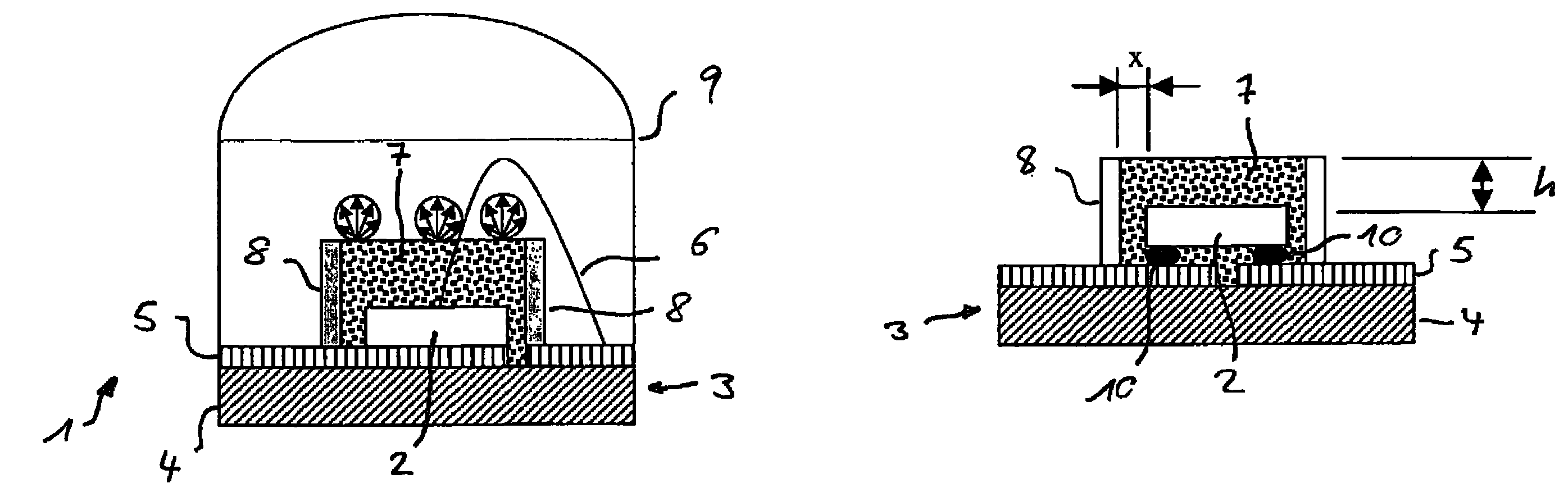
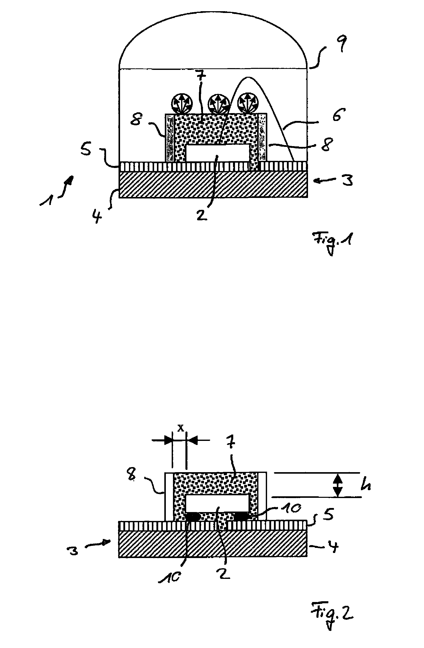
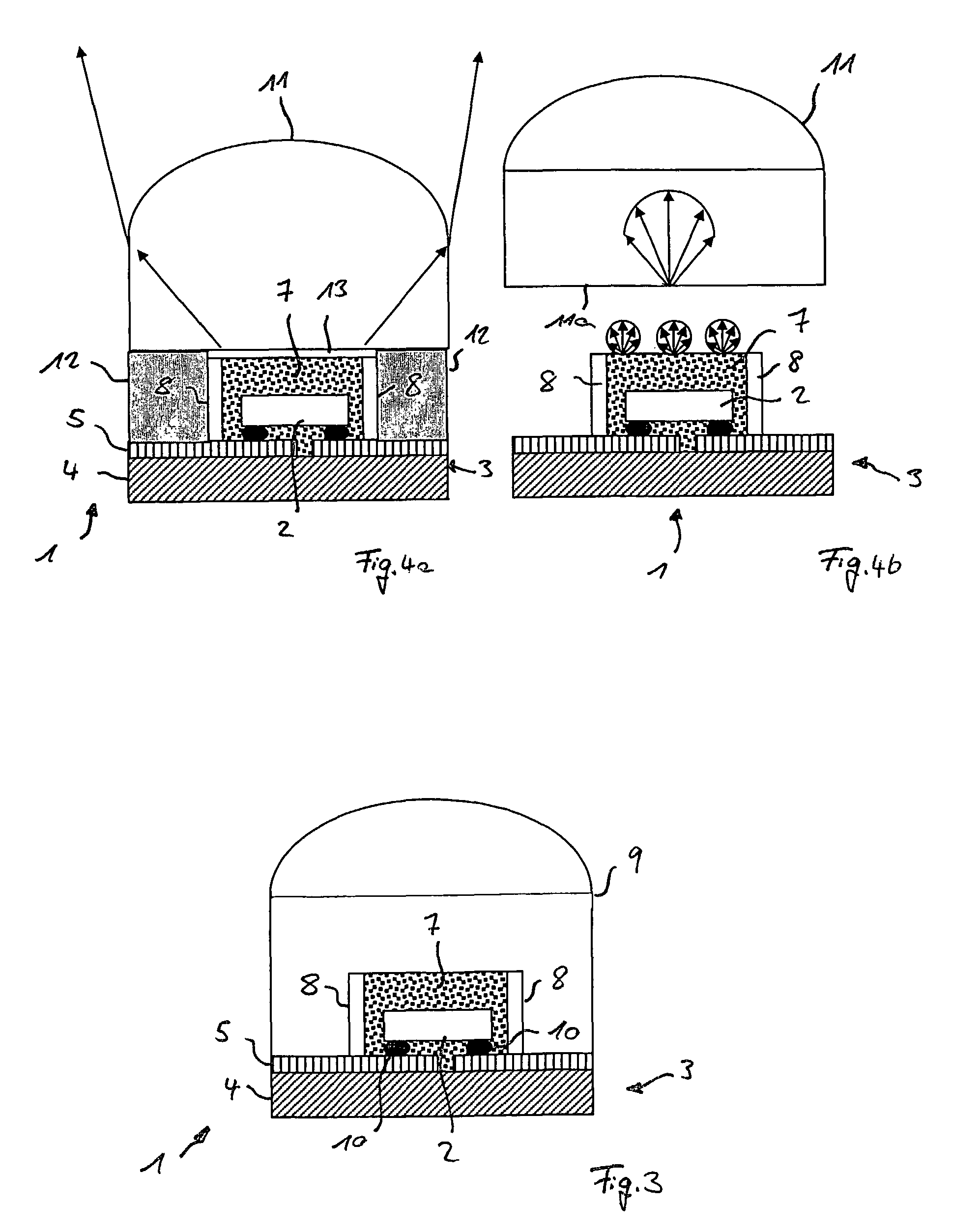
[0032]Firstly the light-emitting diode arrangement illustrated in FIG. 1 and provided with the reference sign 1 has a light-emitting diode chip 2—preferably emitting blue light—which is arranged on a base 3, which has an insulation layer 4 as well as an electrically conductive layer with conductor paths 5, whereby for contacting of the light-emitting diode chip 3 bonding wires lead from these conductors paths to the upper side of the chip. It is to be noted that the base 3 could also be configured in other manner. In particularly specific measures could be taken which make possible an effective heat dissipation from the light-emitting diode chip 2.

[0033]To convert the light emitted by the light-emitting diode chip 2 into a white light mixture, a colour conversion material 7 is provided which surrounds the light-emitting diode chip 2 and has colour conversion particles, in particular phosphors, which convert at least a part of the light into a light of another wavelength. In accordan...


PUM


Abstract

With a light-emitting diode arrangement (1) having a light-emitting diode chip (2) arranged on a base (3), and colour conversion material (7) surrounding the light-emitting diode chip (2), which material is constituted to convert at least a part of the light emitted by the light-emitting diode chip (2) into light of another wavelength, the colour conversion material (7) is surrounded to the side by a reflector (8), the lateral distance (x) of the light-emitting diode chip (2) to the reflector (8) amounting to at most 0.5 mm.

Description

FIELD OF THE INVENTION[0001]The present invention relates to a light-emitting diode arrangement in accordance with the preamble of claim 1 which has a light-emitting diode chip which is surrounded by a colour conversion material which is used to convert at least a part of the light emitted by the light-emitting diode chip into light of another wavelength.BACKGROUND OF THE INVENTION[0002]The field of light-emitting diodes and in particular the field of the so-called “white LEDs” form the background to the present invention. Since light emitting semiconductor elements as a rule emit light at a specific wavelength, the production of a semiconductor element which directly provides white light has not yet been achieved. Instead, the semiconductor elements are configured such that they emit light of an individual wavelength, for example in the colours green, red or blue. To make the generation of white light possible nevertheless, it is known from the state of the art to convert the light...

Claims


Application Information

Patent Timeline
Patent Type & Authority Patents(United States)
IPC IPC(8): H01L29/267H01L29/16H01L33/50H01L33/60
CPCH01L33/505H01L33/60H01L2224/16225H01L2224/48091H01L2924/00014H01L2924/00011H01L2224/0401
Inventor PACHLER, PETER
Owner TRIDONIC OPTOELECTRONICS GMBH
Why Eureka
Try Eureka