Multi-value recording phase-change memory device, multi-value recording phase-change channel transistor, and memory cell array

a memory device and multi-value technology, applied in semiconductor devices, digital storage, instruments, etc., can solve the problems of difficult to achieve multi-value recording, limit the extent to which memory cell density can be increased, etc., to achieve highly reliable multi-value, large margin, and the effect of facilitating the phase-change control of each individual memory layer

Active Publication Date: 2010-08-24
ROHM CO LTD
View PDF10 Cites 3 Cited by
  • Summary
  • Abstract
  • Description
  • Claims
  • Application Information

AI Technical Summary

Benefits of technology

[0012]The present invention has been devised to overcome the above shortcoming associated with the prior art multi-value recording method that uses a phase-change memory device, and an object of the present invention is to provide a novel device structure suitable for multi-value recording, thereby to provide a novel multi-value recording phase-change memory device and multi-value recording phase-change channel transistor having a large margin for the resistance value for multi-value recording and hence capable of achieving multi-value recording with high reliability, and a memory cell formed from such a device or transistor.
[0024]In the multi-value phase-change memory device according to the first invention or the multi-value phase-change channel transistor according to the second invention, since the memory layer formed between the first and second electrodes is constructed from a plurality of mutually isolated sub-memory layers, multi-valued information can be written based on which sub-memory layer or layers are to be caused to change phase. In this case, the change in the resistance value that occurs when one particular sub-memory layer is caused to change phase is almost uniquely determined by the shape of that particular sub-memory layer, and is not affected by the number of phase changes, etc. Accordingly, each individual level of information in the multi-valued information can be written and read out in the form of one of a plurality of clearly distinguished resistance values. This allows a relatively large margin for the writing and reading of multi-valued information, and a highly reliable multi-value phase-change memory device can thus be provided.
[0025]Furthermore, by forming the memory layer in a multilayer structure consisting of a phase-change material layer and a resistive layer, and by setting the resistance value of the resistive layer larger than the resistance value the phase-change material layer exhibits in the crystalline phase, but smaller than the resistance value the phase-change material layer exhibits in the amorphous phase, the write voltage necessary to cause the phase-change material layer to change phase from amorphous to crystalline can be reduced.
[0026]Further, when the plurality of sub-memory layers between the first and second electrode layers are formed so as to have the same resistance value or respectively different resistance values and have respectively different heat capacities, the phase-change control of each individual memory layer becomes further easier.
[0027]Moreover, by constructing a memory cell array by arranging a plurality of such multi-value recording phase-change memory devices or phase-change channel transistors on a single substrate, a memory cell array capable of recording information at higher density can be provided. In particular, when the memory cell array is constructed from multi-value recording phase-change channel transistors, since each switching transistor and its associated memory part, which have had to be formed as separate elements in the prior art, can be implemented in a single transistor, the area each memory cell occupies on the substrate greatly decreases, and thus a memory cell array having a high recording density can be achieved.

Problems solved by technology

There has therefore been a limit to the extent to which memory cell density can be increased.
Accordingly, if the margin for the resistance value is small when recording a 0, a 1, a 2, a 3, etc., multi-value recording becomes difficult to achieve.

Method used


Image

  • Multi-value recording phase-change memory device, multi-value recording phase-change channel transistor, and memory cell array
  • Multi-value recording phase-change memory device, multi-value recording phase-change channel transistor, and memory cell array
  • Multi-value recording phase-change memory device, multi-value recording phase-change channel transistor, and memory cell array

Examples


embodiment 1

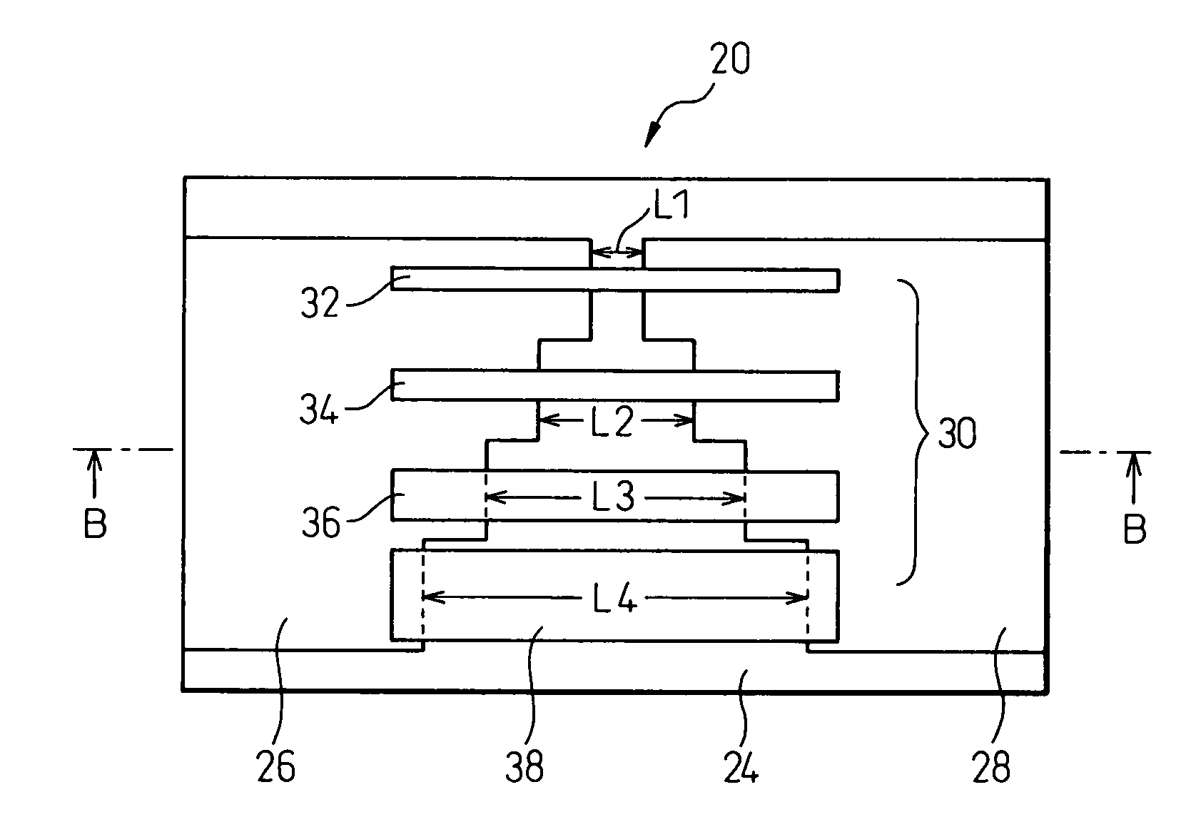
[0047]FIGS. 3(a) and 3(b) are diagrams showing the structure of a phase-change memory device 20 according to a first embodiment of the present invention: Part (a) shows a plan view of the structure and part (b) shows a cross-sectional view taken along line B-B in part (a). As shown, the multi-value recording phase-change memory device 20 according to this embodiment has a structure in which first and second electrode layers 26 and 28 are formed on an insulating film 24 of SiO2 or the like deposited over a semiconductor substrate 22 of Si or the like, and a memory layer 30 of a phase-change material is formed between the electrodes. First and second electrode layers 26 and 28 are current heating electrodes for memory layer 30 and are formed from Al, Au, or like material. The opposing side faces of first and second electrode layers 26 and 28 are each formed in a staircase shape so that the distance L (L1, L2, L3, L4) between the electrodes changes in a step-like manner.

[0048]Memory la...

embodiment 2

[0057]FIG. 4 is a diagram showing the structure of a multi-value recording phase-change memory device 20A according to a second embodiment of the present invention: Part (a) of the figure shows a plan view of the structure and part (b) shows a cross-sectional view taken along line B-B in part (a). In the drawings given hereinafter, the same reference numerals as those in FIG. 3 designate identical or similar component elements to those described with reference to FIG. 3, and therefore, such component elements will not be further described herein.

[0058]Memory layer 30A of this embodiment comprises sub-memory layers 32A, 34A, 34A, and 38A. Each of sub-memory layers 32A, 34A, 34A, and 38A has a two-layer structure consisting of a phase-change material layer (34a) and a resistive layer (34b), as represented, for example, by sub-memory layer 34A in FIG. 4(b). In sub-memory layers 32A to 38A, since the phase-change material layers (indicated by 34a in the case of sub-memory layer 34) are ...

embodiment 3

[0063]FIG. 5 is a diagram showing the structure of a multi-value recording phase-change channel transistor 50 according to a third embodiment of the present invention: Part (a) of the figure shows a plan view of the structure and part (b) shows a cross-sectional view taken along line C-C in part (a). In this transistor 50, memory layer 40 comprises sub-memory layers 42, 44, 46, and 48, which are formed from the same material and in the same shape as sub-memory layers 32A, 34A, 36A, and 38A shown in FIG. 4. However, transistor 50 of the present embodiment differs from the phase-change memory of FIG. 4 in that, in each of sub-memories 42, 44, 46, and 48, a gate electrode 52 is formed on top of the phase-change material layer (for example, 44a) by interposing an insulating layer (for example, 44c) therebetween. In FIG. 5(b), a multilayer structure consisting of resistive layer 44b, phase-change material layer 44a, and insulating layer 44c is shown only for sub-memory layer 44, but it i...


PUM


Abstract

A multi-value recording phase-change memory device that can stably record multi-value information, and that can reproduce information with high reliability, comprises a first electrode layer 26, a second electrode layer 28, and a memory layer 30 provided between the first and second electrode layers 26 and 28 and containing a phase-change material layer formed from a phase-change material which is stable in either an amorphous phase or a crystalline phase at room temperature, wherein the memory layer 30 includes a plurality of mutually isolated sub-memory layers 32, 34, 36, and 38 between the first and second electrode layers 26 and 28.

Description

CROSS-REFERENCE TO RELATED APPLICATION[0001]This application claims priority from Japanese Patent Application No. 2006-271743, filed on Oct. 3, 2006.TECHNICAL FIELD OF THE INVENTION[0002]The present invention relates to a multi-value recording phase-change memory device and a multi-value recording phase-change channel transistor, each using a phase-change material which is stable in either a crystalline phase or an amorphous phase at room temperature, and also relates to a memory cell array constructed from such devices or transistors.BACKGROUND OF THE INVENTION[0003]A chalcogenide-based material, for example, has the property of being stable in either a crystalline phase or an amorphous phase at room temperature, and its resistivity changes by two to four orders of magnitude between the two phases. A nonvolatile memory is realized by making use of this property. In other words, information is written by causing a thin film of such a material to stabilize in either the crystalline o...

Claims


Application Information

Patent Timeline
Patent Type & Authority Patents(United States)
IPC IPC(8): H01L29/02
CPCG11C11/5678H01L27/2436H01L45/06H01L45/1226H01L45/144H01L45/148G11C13/0004H10B63/30H10N70/823H10N70/884H10N70/231H10N70/8828
Inventor HOSAKA, SUMIOSONE, HAYATOYOSHIMARU, MASAKIONO, TAKASHINAKASATO, MAYUMI
Owner ROHM CO LTD
Why Eureka
Try Eureka