Ultrasonic probe and method of manufacturing the same

a technology of ultrasonic probes and manufacturing methods, applied in the field of ultrasonic probes, can solve the problems of physical weakness of side electrodes, and achieve the effects of improving yield, and reducing the difficulty level of manufacturing

Active Publication Date: 2010-09-14
FUJIFILM CORP
View PDF5 Cites 7 Cited by
  • Summary
  • Abstract
  • Description
  • Claims
  • Application Information

AI Technical Summary

Benefits of technology

[0015]The present invention has been achieved in view of the above-mentioned problems. A purpose of the present invention is, in an ultrasonic probe including plural multilayered piezoelectric elements, in the case where individual wires led out from the multilayered piezoelectric elements are arranged in a staggered manner, to prevent short-circuit to side electrodes of the multilayered piezoelectric elements caused if a conducting adhesive flows out when the individual wires are bonded. A further purpose of the present invention is to improve mechanical strength of the side electrodes.
[0018]According to one aspect of the present invention, since the insulating film electrically separates the second side electrode and the conducting adhesive material in the first multilayered piezoelectric element, the short-circuit to side electrodes of the multilayered piezoelectric elements caused if the conducting adhesive flows out when the individual wires are bonded can be prevented. As a result, the difficulty level of working at manufacturing can be reduced and the yield can be improved. Further, the side electrodes are physically weak, but the resistance to the mechanical damage in manufacturing can be provided when the side electrodes are covered by the insulating film.

Problems solved by technology

Further, the side electrodes are physically weak, but the resistance to the mechanical damage in manufacturing can be provided when the side electrodes are covered by the insulating film.

Method used


Image

  • Ultrasonic probe and method of manufacturing the same
  • Ultrasonic probe and method of manufacturing the same
  • Ultrasonic probe and method of manufacturing the same

Examples


first embodiment

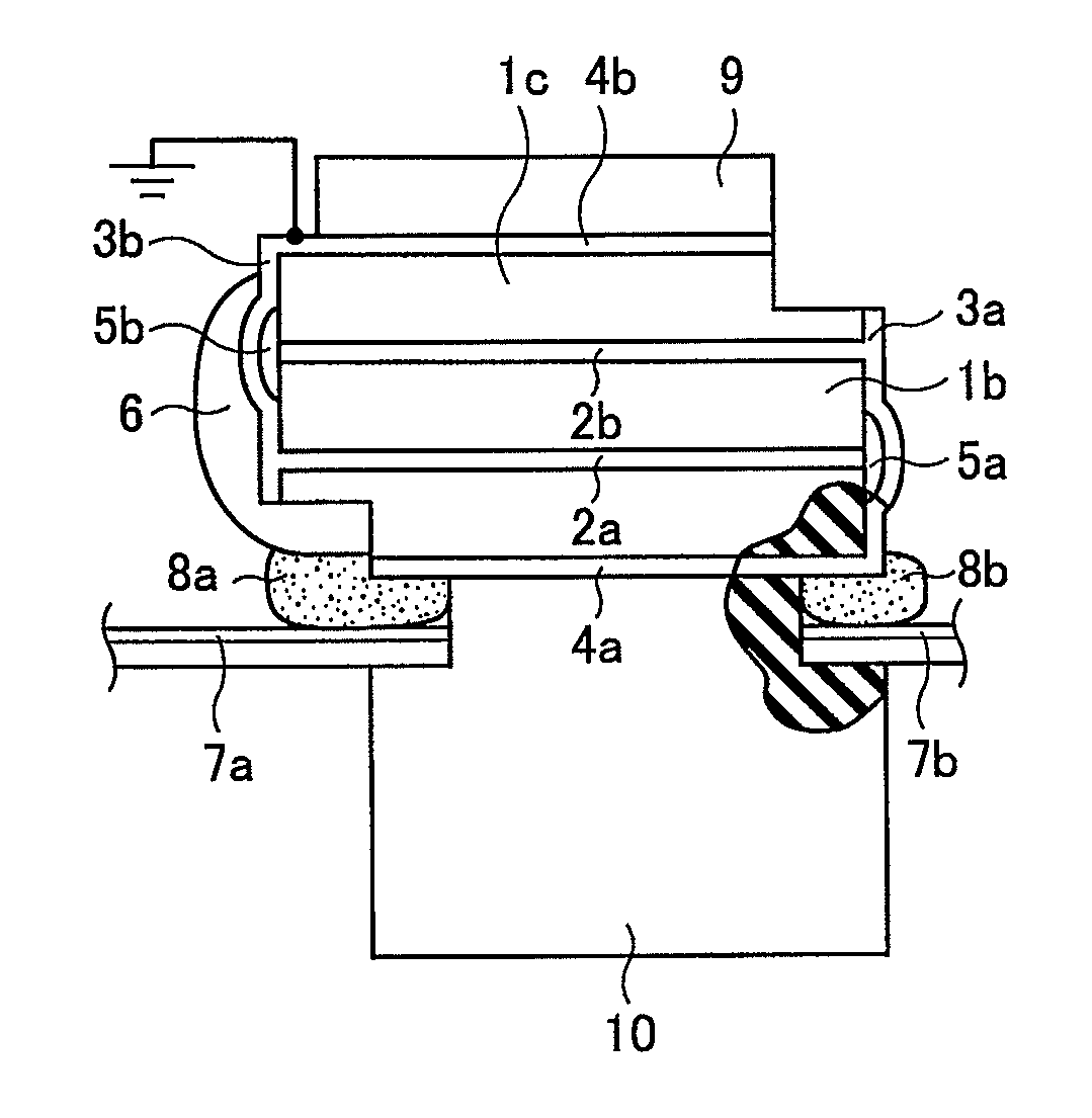
[0028]FIG. 1 shows an internal structure of an ultrasonic probe according to the present invention. In FIG. 1, (a) is a front view, (b) is a left-side view, and (c) is a right-side view.

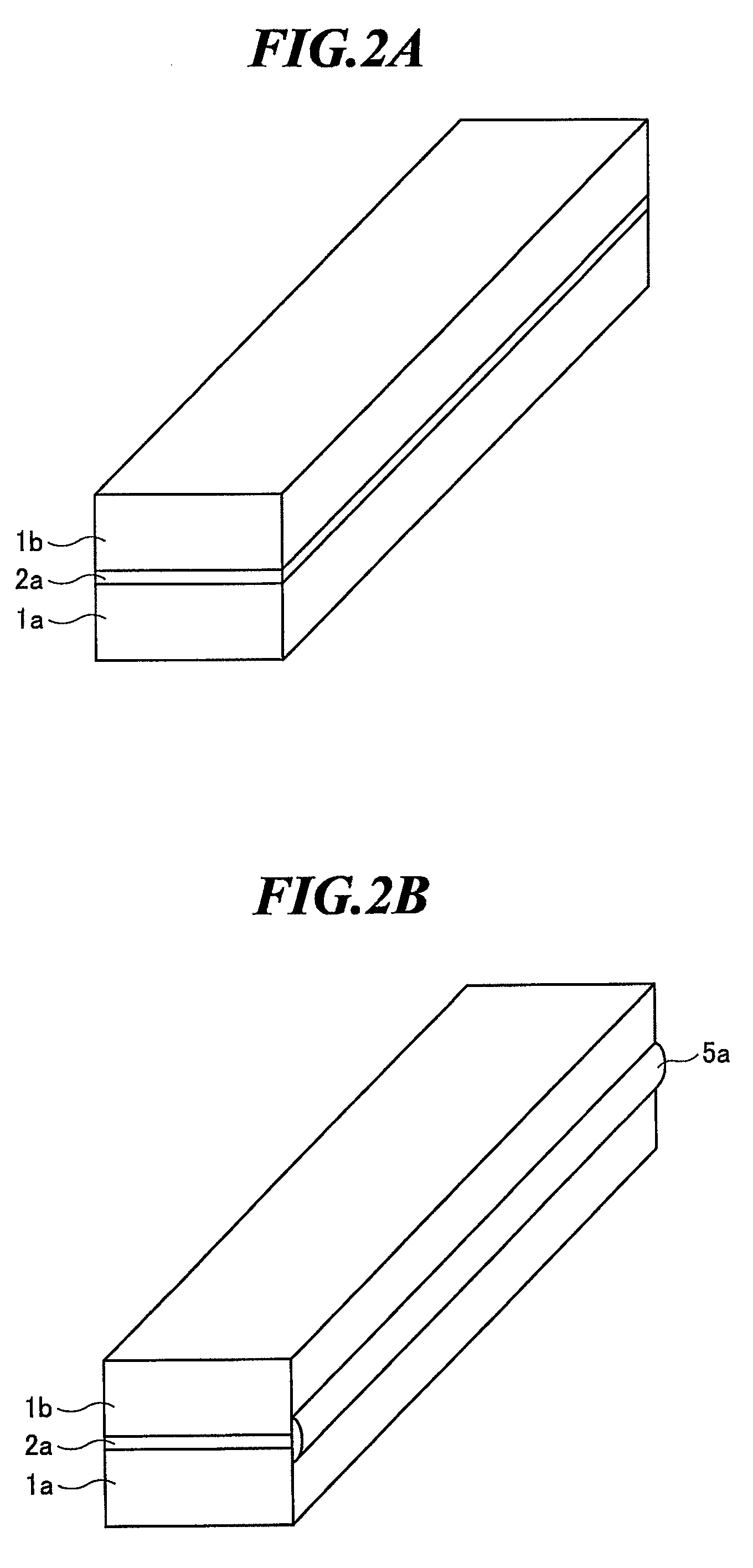
[0029]The ultrasonic probe includes plural multilayered piezoelectric elements 11a and 11b arranged in a row. Each of the multilayered piezoelectric elements has a multilayered structure in which plural piezoelectric layers 1a and 1b and at least one internal electrode 2a are alternately stacked, a flat electrode 4a formed on the piezoelectric layer 1a located at the lower end of the multilayered structure, a flat electrode 4b formed on the piezoelectric layer 1b located at the upper end of the multilayered structure, an insulating film 5a formed on the right side surface of the multilayered structure, a side electrode 3a formed on the right side surface of the multilayered structure and connected to odd-numbered electrodes of the flat electrodes 4a and 4b and the at least one internal electrode 2a, ...

second embodiment

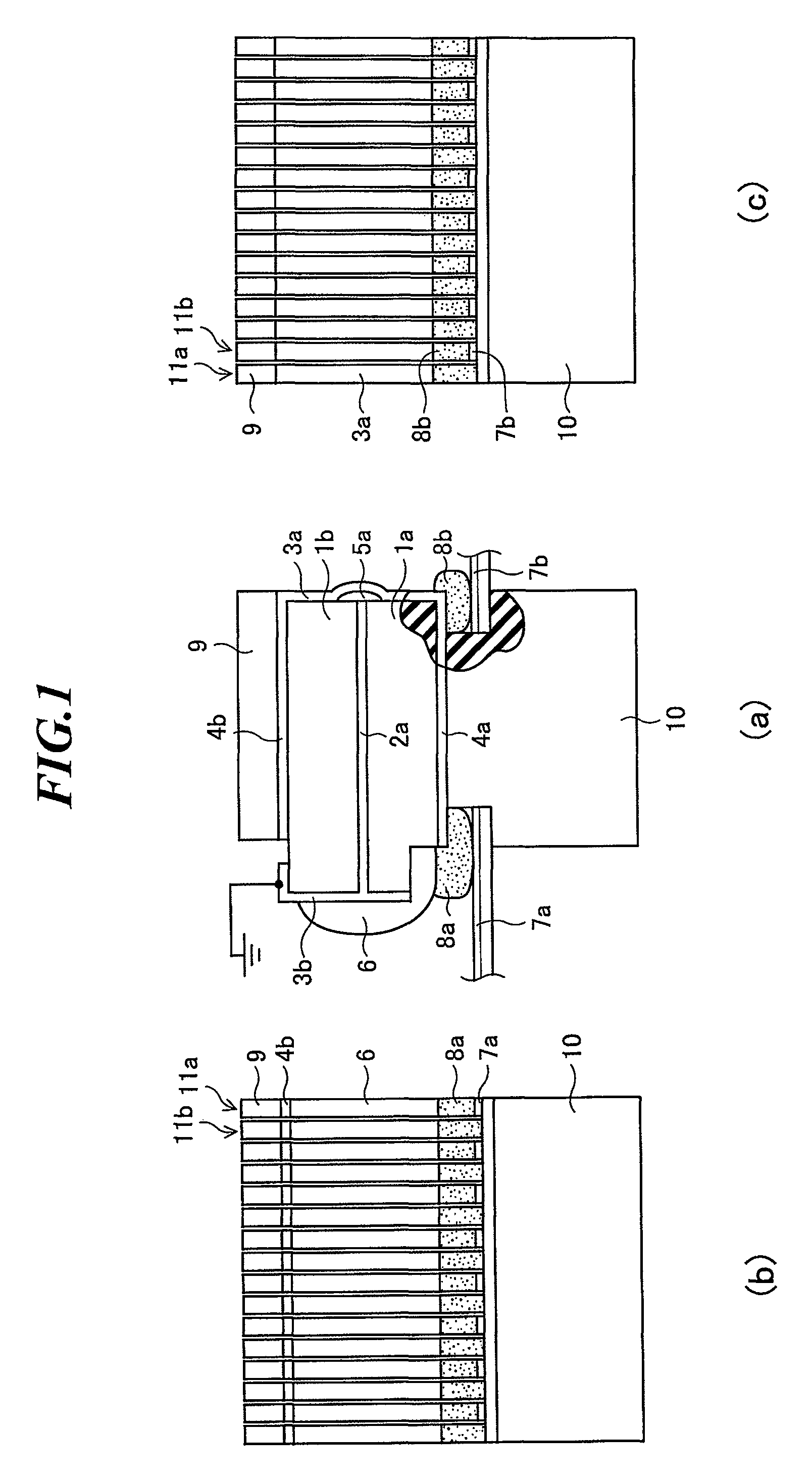
[0046]FIG. 3 is a front view showing an ultrasonic probe according to the present invention. As shown in FIG. 3, as the third piezoelectric material layer, a piezoelectric material layer 1c is provided on the piezoelectric material layer 1b via an internal electrode 2b. An insulating film 5b is formed on the end of the internal electrode 2b at the side electrode 3b side, and the internal electrode 2b is electrically connected to the side electrode 3a and electrically insulated from the side electrode 3b. Further, a notch part (groove) that cuts the side electrode 3a side in the array arrangement direction is provided in the flat electrode 4b and the piezoelectric material layer 1c. Accordingly, the flat electrode 4b is electrically connected to the side electrode 3b and electrically insulated from the side electrode 3a. Thereby, the same electric field as that for the piezoelectric material layer 1a is applied to the piezoelectric material layer 1c.

[0047]In this manner, in the case...

third embodiment

[0049]FIG. 4 is a front view showing an ultrasonic probe according to the present invention. As shown in FIG. 4, an insulating film 5c of an insulating resin is provided inside of the end part of the side electrode 3a at the flat electrode 4b, and an insulating film 5d of the insulating resin is provided inside of the end part of the side electrode 3b at the flat electrode 4a.

[0050]The insulating film 6 covers the corner part where the side electrode 3b and the flat electrode 4a are separated by the insulating film 5d. In the third embodiment, the end part of the side electrode 3b at the flat electrode 4a side is covered by the insulating film 6, and the short-circuit of the conducting adhesive material 8a to the side electrode 3b can be prevented.

[0051]Next, the fourth embodiment of the present invention will be explained. In the first to third embodiments, the example of multilayered structure of whole surface electrode structure has been shown, however, in the fourth embodiment,...


PUM

PropertyMeasurementUnit
thicknessaaaaaaaaaa
thicknessesaaaaaaaaaa
thicknessaaaaaaaaaa

Abstract

In an ultrasonic probe in which individual wires led out from multilayered piezoelectric elements are arranged in a staggered manner, short-circuit is prevented. Each of the elements includes: a multilayered structure in which piezoelectric material layers and at least one internal electrode are stacked; first and second flat electrodes; first and second side electrodes; an insulating film formed at a second side surface side of the multilayered structure; a wiring member bonded to the first flat electrode on the one end of the multilayered structure by using a conducting adhesive material; and the wiring member is provided at the second side surface side of the multilayered structure and the insulating film electrically separates the second side electrode and the conducting adhesive material in a first element, and the wiring member is provided at a first side surface side of the multilayered structure in a second element.

Description

BACKGROUND OF THE INVENTION[0001]1. Field of the Invention[0002]The present invention relates to an ultrasonic probe including plural ultrasonic transducers for transmitting and / or receiving ultrasonic waves in an ultrasonic diagnostic apparatus for medical use or structure flaw detection, and a method of manufacturing such an ultrasonic probe.[0003]2. Description of a Related Art[0004]In medical fields, various imaging technologies have been developed in order to observe the interior of an object to be inspected and make diagnoses. Especially, ultrasonic imaging for acquiring interior information of the object by transmitting and receiving ultrasonic waves enables image observation in real time without exposure to radiation like other medical image technologies such as X-ray photography or RI (radio isotope) scintillation camera. Accordingly, ultrasonic imaging is utilized as an imaging technology at a high level of safety in a wide range of departments including not only the fetal...

Claims


Application Information

Patent Timeline
Patent Type & Authority Patents(United States)
IPC IPC(8): H01L41/047H01L41/083A61B8/00B06B1/06G01N29/24H02N2/00H04R17/00H04R31/00
CPCB06B1/064G01N29/2437Y10T29/42
Inventor NAKAYAMA, RYUICHIOSAWA, ATSUSHI
Owner FUJIFILM CORP
Why Eureka
Try Eureka