Non-volatile semiconductor storage device

a non-volatile, semiconductor technology, applied in semiconductor devices, digital storage, instruments, etc., can solve the problems of difficult reduction of writing voltage, inability to reduce the number of hv-type transistors, and inability to shrunken hv-type transistors

Active Publication Date: 2010-09-21
KIOXIA CORP
View PDF5 Cites 133 Cited by
  • Summary
  • Abstract
  • Description
  • Claims
  • Application Information

AI Technical Summary

Problems solved by technology

However, such HV-type transistors cannot be shrunken since it is difficult to decrease writing voltage.
Furthermore, for example, the HV-type transistors are required as many as word lines because they are provided in row decoder circuits connected to the word lines, and hence the number of HV-type transistors cannot be reduced.
Therefore, these HV-type transistors form bottlenecks for the entire chip, causing problems that the chip size cannot be shrunken.

Method used


Image

  • Non-volatile semiconductor storage device
  • Non-volatile semiconductor storage device
  • Non-volatile semiconductor storage device

Examples


first embodiment

General Configuration of Non-Volatile Semiconductor Storage Device According to First Embodiment

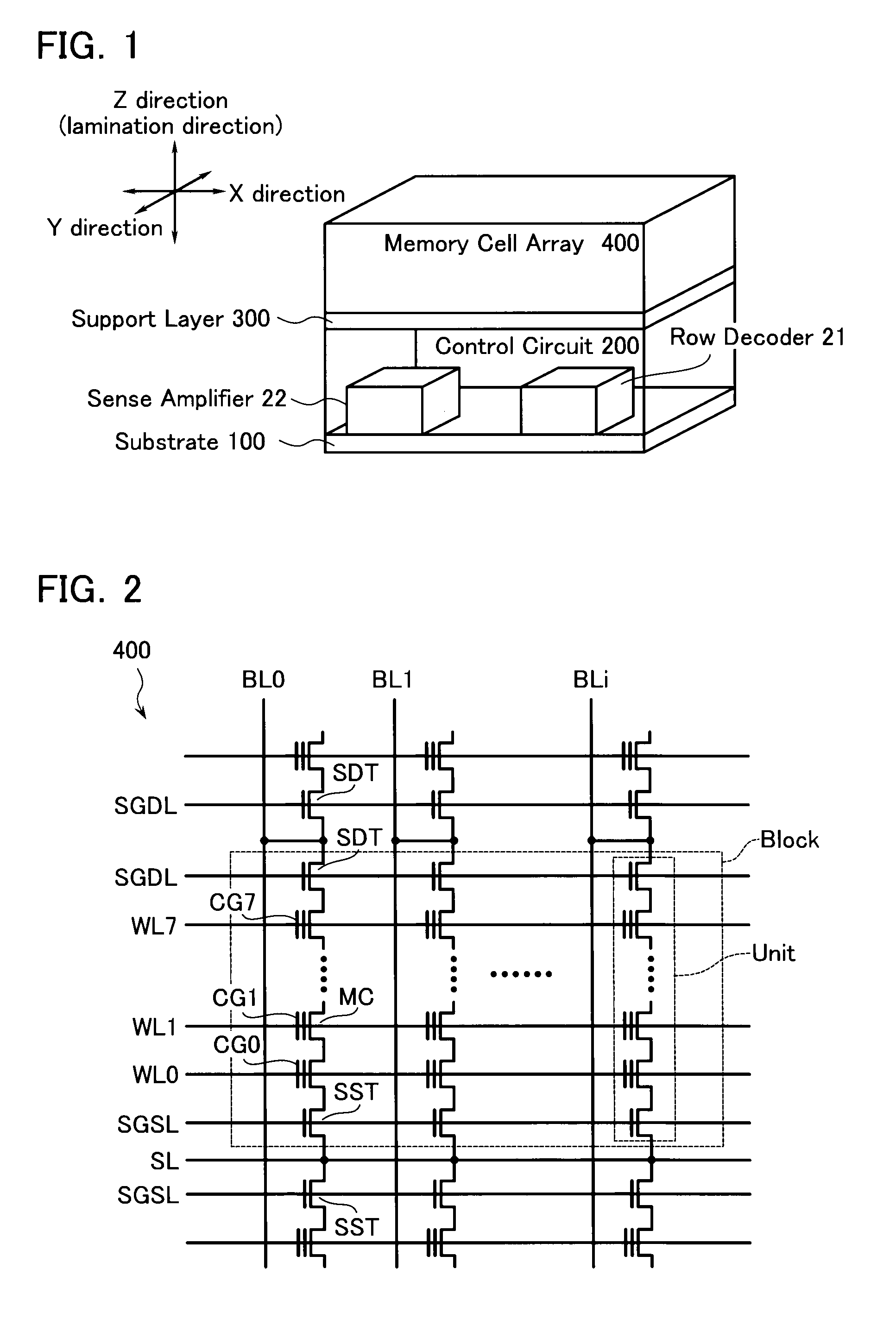
[0038]FIG. 1 is a schematic diagram of a non-volatile semiconductor storage device according to a first embodiment of the present invention. As illustrated in FIG. 1, the non-volatile semiconductor storage device according to the first embodiment has a substrate 100; a control circuit 200 provided on the substrate 100; a support layer 300 provided on the control circuit 200; and a memory cell array 400 provided on the support layer 300.

[0039]The control circuit 200 has a function for controlling the operation of the memory cell array 400. The control circuit 200 includes a row decoder 21, a sense amplifier 22, etc. The row decoder 21 drives the potentials of word lines WL to “H (high level)” or “L (low level)” that are provided in the memory cell array 400 (see FIG. 2, discussed below). The sense amplifier 22 senses and amplifies signals from bit lines BL in the memory cell array 400 (see...

second embodiment

Specific Configuration of Non-Volatile Semiconductor Storage Device According to Second Embodiment

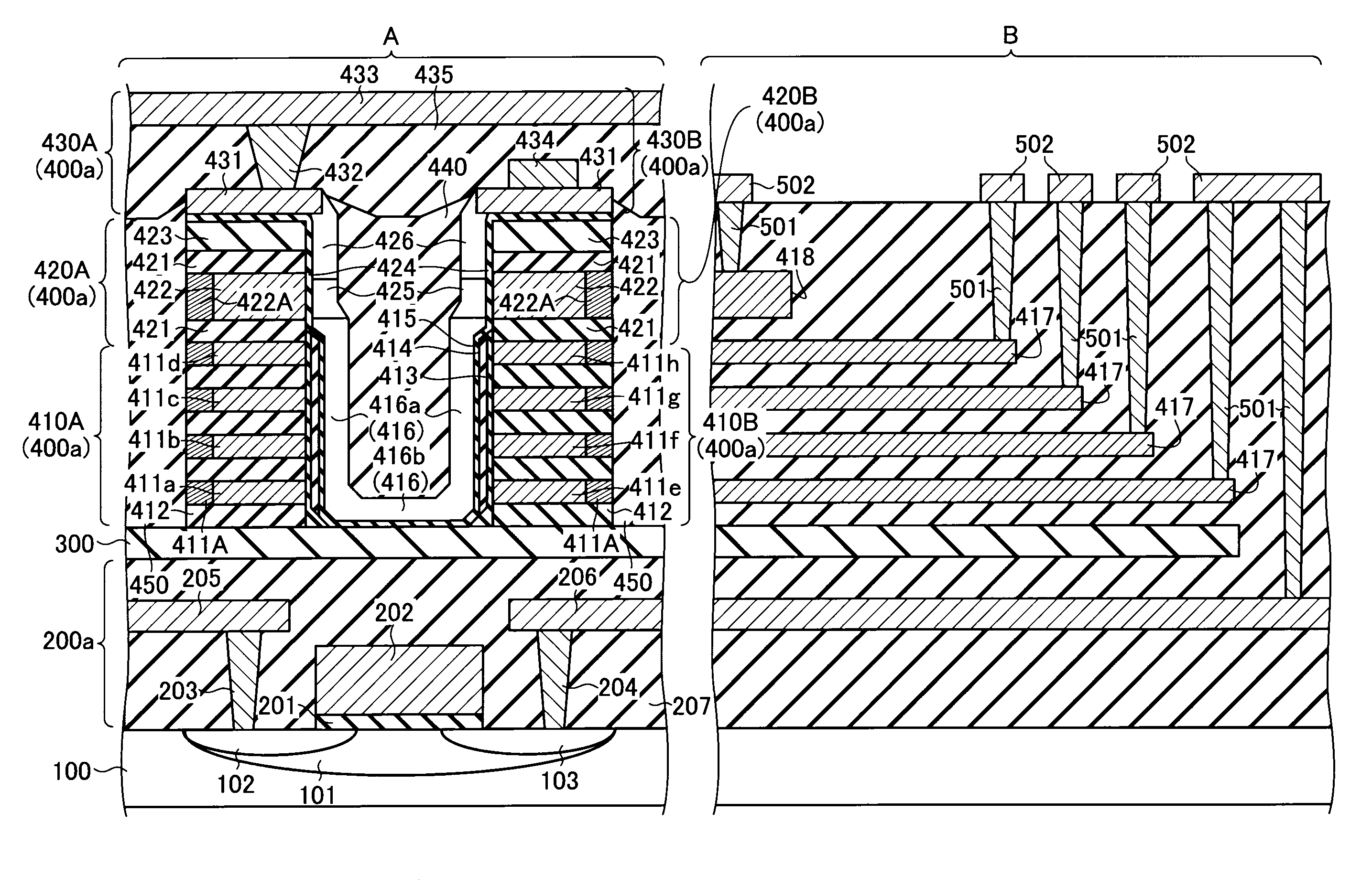
[0093]Referring now to FIG. 15, a specific configuration of a non-volatile semiconductor storage device according to a second embodiment of the present invention will be described below. As illustrated in FIG. 15, the non-volatile semiconductor storage device according to the second embodiment has a control circuit layer 200b different than the first embodiment. Note that the same referent numerals represent the same components as the first embodiment and description thereof will be omitted in the second embodiment.

[0094]As illustrated in FIG. 15, the control circuit layer 200b has insulation layers 211 that are provided on the top surface of the substrate 100, gate conductive layers 202 that are provided on the top surfaces of the insulation layers 211, and wiring layers 213 that are provided on the top surfaces of the insulation layers 211.

[0095]Each of the insulation layers 211 has a...

third embodiment

Specific Configuration of Non-Volatile Semiconductor Storage Device According to Third Embodiment

[0099]Referring now to FIG. 16, a specific configuration of a non-volatile semiconductor storage device according to a third embodiment of the present invention will be described below. As illustrated in FIG. 16, the non-volatile semiconductor storage device according to the third embodiment has a memory array layer 400b different than the first embodiment. Note that the same reference numerals represent the same components as the first embodiment and description thereof will be omitted in the third embodiment.

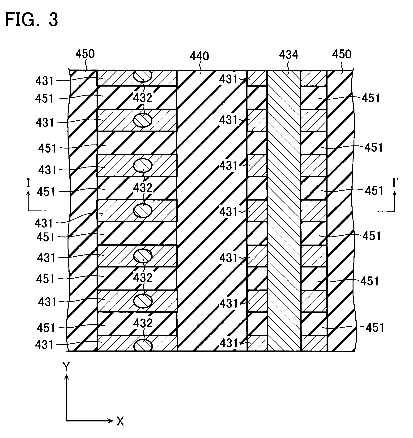
[0100]As illustrated in FIG. 16, the non-volatile semiconductor storage device according to the third embodiment is different than the first embodiment in the configurations of the support layer 300, the first lamination parts 410A and 410B, and the third lamination parts 430A and 430B. In addition, fourth lamination parts 460A and 460B are formed between the first lamination parts...


PUM


Abstract

A non-volatile semiconductor storage device includes: a substrate; a control circuit layer provided on the substrate; a support layer provided on the control circuit layer; and a memory cell array layer provided on the support layer. The memory cell array layer includes: a first lamination part having first insulation layers and first conductive layers alternately laminated therein; and a second lamination part provided on either the top or bottom surface of the respective first lamination part and laminated so as to form a second conductive layer between second insulation layers. The control circuit layer includes at least any one of: a row decoder driving word lines provided in the memory cell array layer, and a sense amplifier sensing and amplifying a signal from bit lines provided in the memory cell array layer.

Description

CROSS-REFERENCE TO RELATED APPLICATIONS[0001]This application is based upon and claims the benefit of priority from the prior Japanese Patent Application No. 2007-262430, filed on Oct. 5, 2007, the entire contents of which are incorporated herein by reference.BACKGROUND OF THE INVENTION[0002]1. Field of the Invention[0003]The present invention relates to an electrically rewritable non-volatile semiconductor storage device and a method of manufacturing the same.[0004]2. Description of the Related Art[0005]Recently, the number of bits (the number of transistors) tends to increase for the purpose of providing a larger amount of data to be written to one chip. This is achieved by shrinking the transistor size. On the other hand, for EEPROM using high voltage in writing or the like, HV-type transistors are essential that are durable for such high voltage. For example, non-volatile semiconductor devices includes two regions: a memory cell array arranging region, and a periphery region tha...

Claims


Application Information

Patent Timeline
Patent Type & Authority Patents(United States)
IPC IPC(8): H01L27/115
CPCH01L27/115H01L27/11568H01L27/11578H01L27/11582H10B43/30H10B69/00H10B43/20H10B43/27
Inventor IZUMI, TATSUOKAMIGAICHI, TAKESHI
Owner KIOXIA CORP
Why Eureka
Try Eureka