Method of forming a vertical diode and method of manufacturing a semiconductor device using the same

a technology of vertical diodes and semiconductor devices, applied in the direction of diodes, semiconductor devices, electrical devices, etc., can solve the problems of affecting the operation of flash memory devices, the active region exposed by the opening may be damaged, and the driving current capacity of transistors is not greater than about 1 ma, so as to achieve stable driving current

Active Publication Date: 2010-09-28
SAMSUNG ELECTRONICS CO LTD
View PDF10 Cites 8 Cited by
  • Summary
  • Abstract
  • Description
  • Claims
  • Application Information

AI Technical Summary

Benefits of technology

[0011]Example embodiments of the present invention can be characterized as providing a method of forming a vertical diode ensuring a stable driving current.
[0012]Example embodiments of the present invention can also be characterized as providing a method of manufacturing a semiconductor device (e.g., a semiconductor memory device such as a phase-change memory device) using the method of forming the vertical diode ensuring the stable driving current.

Problems solved by technology

However, it may take a relatively long time to input / output data into / from a flash memory device.
However, when the transistor is used as the switching element, the transistor may not have a driving current capacity greater than about 1 mA, which is required for a phase-transition of the phase-change material layer.
However, when the insulation layer is patterned to form the insulation layer pattern having the opening, the active region exposed by the opening may be damaged.
Due to the damage to the active region or the interface stress, it may not be easy to form a polysilicon layer having a gross grain size.
However, the heat treatment process is usually performed at a temperature higher than about 600° C. As a result, the crystalline characteristics of the polysilicon layer may be inferior compared to the crystalline characteristics of a polysilicon layer formed by the SEG process.

Method used


Image

  • Method of forming a vertical diode and method of manufacturing a semiconductor device using the same
  • Method of forming a vertical diode and method of manufacturing a semiconductor device using the same
  • Method of forming a vertical diode and method of manufacturing a semiconductor device using the same

Examples


Embodiment Construction

[0021]Example embodiments of the present invention are described more fully hereinafter with reference to the accompanying drawings. These example embodiments may, however, be realized in many different forms and should not be construed as limited to the example embodiments set forth herein. Rather, these example embodiments are provided so that this disclosure will be thorough and complete, and will fully convey the scope of the present invention to those skilled in the art. In the drawings, the sizes and relative sizes of layers and regions may be exaggerated for clarity.

[0022]It will be understood that when an element or layer is referred to as being “on” or “connected to” another element or layer, it can be directly on, connected or coupled to the other element or layer or intervening elements or layers may be present. In contrast, when an element is referred to as being “directly on” or “directly connected to” another element or layer, there are no intervening elements or layer...


PUM

PropertyMeasurementUnit
temperatureaaaaaaaaaa
driving current capacityaaaaaaaaaa

Abstract

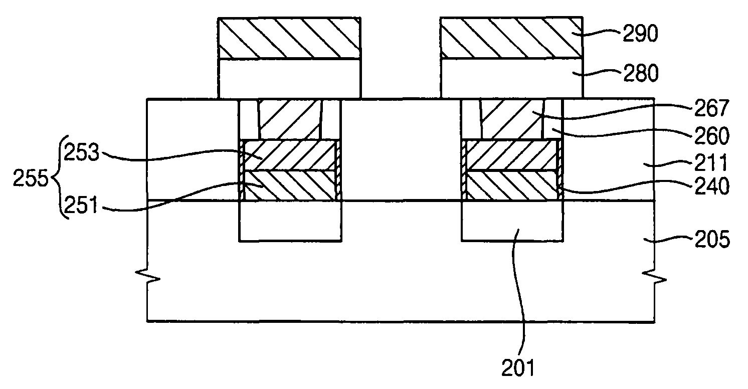
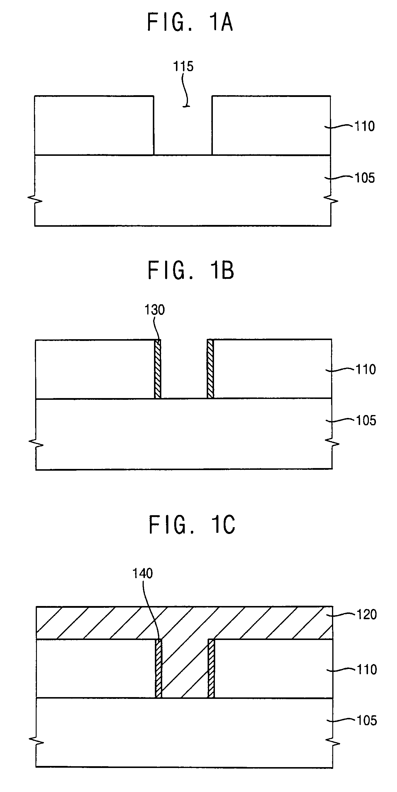
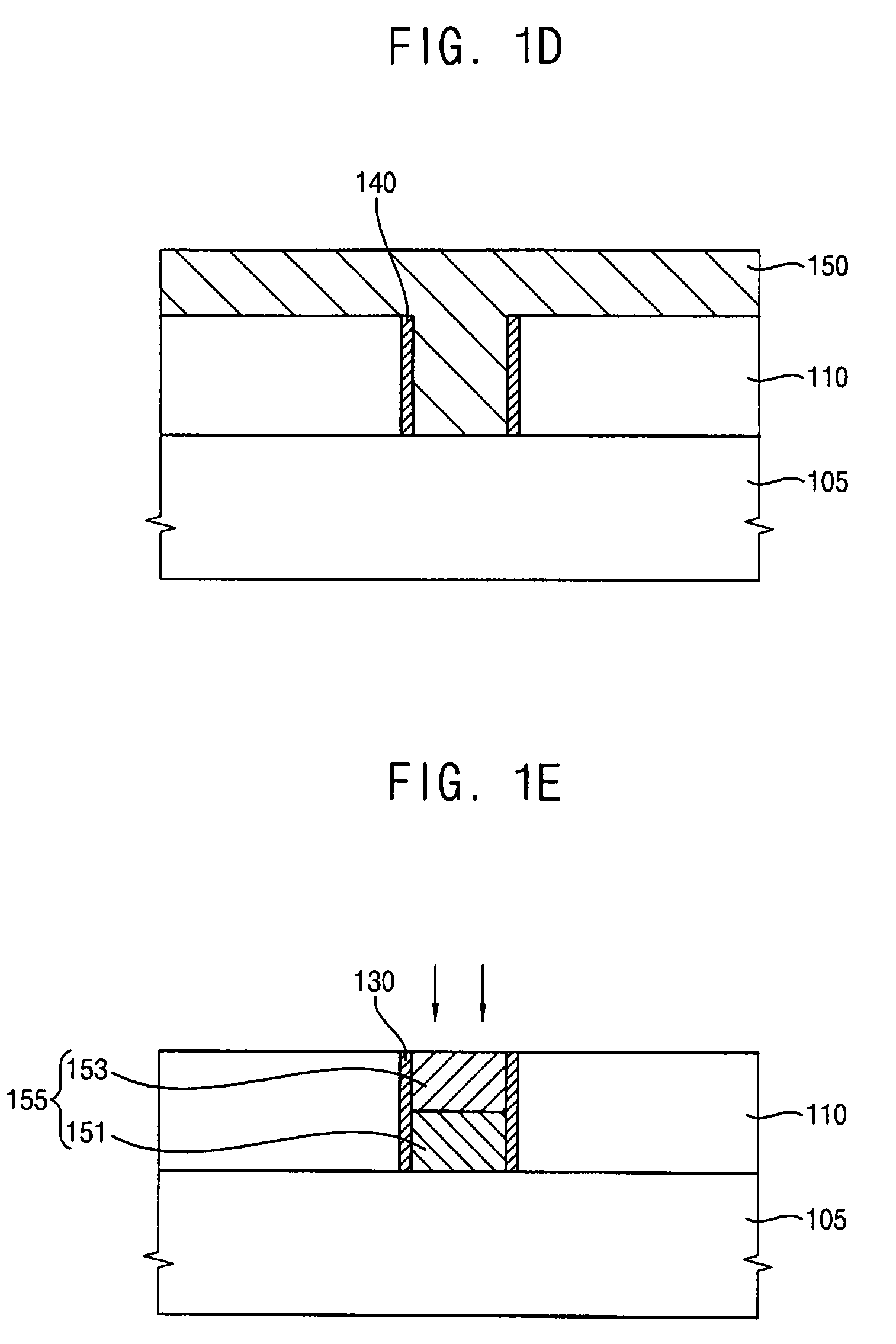
A method of forming a vertical diode and a method of manufacturing a semiconductor device (e.g., a semiconductor memory device such as a phase-change memory device) includes forming an insulating structure having an opening on a substrate and filling the opening with an amorphous silicon layer. A metal silicide layer is formed to contact at least a portion of the amorphous silicon layer and a polysilicon layer is then formed in the opening by crystallizing the amorphous silicon layer using the metal silicide layer. A doped polysilicon layer is formed by implanting impurities into the polysilicon layer. Thus, the polysilicon layer is formed in the opening without performing a selective epitaxial growth (SEG) process, so that electrical characteristics of the diode may be improved.

Description

CROSS-REFERENCE TO RELATED APPLICATION[0001]This application claims priority under 35 USC §119 to Korean Patent Application No. 2007-17451, filed on Feb. 21, 2007, the contents of which are herein incorporated by reference in their entirety.BACKGROUND[0002]1. Field of Invention[0003]Embodiments of the present invention relate to methods of forming a diode and methods of manufacturing a semiconductor device (e.g., a semiconductor memory device such as a phase-change memory device) using the same. More particularly, embodiments of the present invention relate to a method of forming a vertical diode in which a polysilicon layer may be formed at a relatively low temperature, and a method of manufacturing a semiconductor device using the same.[0004]2. Description of the Related Art[0005]Generally, semiconductor memory devices can be classified as either volatile semiconductor memory devices or non-volatile semiconductor memory devices. Volatile semiconductor memory devices include dynami...

Claims


Application Information

Patent Timeline
Patent Type & Authority Patents(United States)
IPC IPC(8): H01L29/88
CPCH01L21/0237H01L21/02488H01L21/02532H01L21/02667H01L21/02672H01L27/2409H01L29/66136H01L29/66204H01L45/06H01L45/1233H01L45/143H01L45/144H01L45/1675H01L27/1021H10B63/20H10N70/8825H10N70/231H10N70/8828H10N70/063H10N70/826H01L29/861H10B99/00
Inventor PARK, SANG-JINLEE, KONG-SOOHYUNG, YONG-WOOYOU, YOUNG-SUBHAN, JAE-JONG
Owner SAMSUNG ELECTRONICS CO LTD
Why Eureka
Try Eureka