Adjustable low-loss interface

a low-loss, adjustable technology, applied in the field of interfaces, can solve the problems of affecting the quality of the interface, the loss of a large portion of the signal as it travels through the circuit, and the loss of metals,

Active Publication Date: 2010-10-12
VIASAT INC
View PDF32 Cites 192 Cited by
  • Summary
  • Abstract
  • Description
  • Claims
  • Application Information

AI Technical Summary

Benefits of technology

[0011]In general, in accordance with one exemplary aspect of the present invention, an interface is disclosed for connecting two devices where energy is transmitted or received there between. In one exemplary embodiment, the interface of the present invention is a low-loss interface that directly connects a MMIC to a waveguide without the use of dielectric materials. Further, according to one exemplary embodiment, the interface further comprises an isolation wall located between an input region and output region of one of the devices that transmits or receives energy. In yet another exemplary embodiment, a turning screw or other adjustable member is provided to increase or decrease the cavity volume within the interface and / or the waveguide cavity to most closely match the impedance at the connection point between the circuit and interface.

Problems solved by technology

Transitioning microwave signals from one mode to another or interfacing to another medium is “lossy.” By being lossy, a portion of the signal is lost as it travels through the circuits, wires, and other mediums.
Transitions at microwave frequencies are particularly difficult and lossy.
At microwave frequencies metal losses become greater due to reduced skin depth and increased sensitivity to surface roughness.
Apart from materials being lossier at microwave frequencies, the design of the transitions and interfaces is more difficult.
It is difficult to control or predict phase at microwave frequencies.
This leads to greater mismatch losses.
One exemplary circuit that generates and transports microwaves is a “monolithic microwave integrated circuit” or “MMIC.” Lost signal waves are unusable and decrease the efficiency of a MMIC as the signal strength decreases due to loss.
Generally, the higher the frequency of the microwave, the more lossy the transmission medium and more inefficient the circuit.
In certain applications, even signal losses that reduce the signal small amounts, such as 1 / 10 of a decibel, may result in a significant performance loss.
Unfortunately, signal loss is still problematic with certain waves because the connection or interface between the circuit generating the energy waves and the waveguide can be lossy itself.
The interfaces between a waveguide and an integrated circuit tend to be lossy in part, due to the initial transition from a circuit such as a MMIC to the interface.
This initial transition between an integrated circuit and an interface is lossy due to the impedance difference between the integrated circuit and interface.
MMICs have some of the greatest and most noticeable amounts of signal loss due to due to the types of interfaces used to connect MMICs to other energy transmission devices, such as waveguides.
Moreover, impedance miss-matches from the MMIC to the waveguide enhance signal losses.
Throughout, the term “interface” is meant to denote an “impedance matching interface” or “impedance matching and transforming interface.” However, current impendence matching interfaces between an integrated circuit such as a MMIC and a waveguide still have an unacceptable amount of loss.
Much of this loss is due to the extra components such as microstrips, suspended strip lines and pins that result in higher loss.
Besides lossiness, MMICs and other similar circuits suffer from an excess of “ripple.” Ripple is unwanted gain variation versus frequence due to the mismatch of impedances at two electronic devices, such as a microstrip track and MMIC or from a microstrip to a suspended stripline or from a suspended stripline to a waveguide.

Method used


Image

  • Adjustable low-loss interface
  • Adjustable low-loss interface
  • Adjustable low-loss interface

Examples


Embodiment Construction

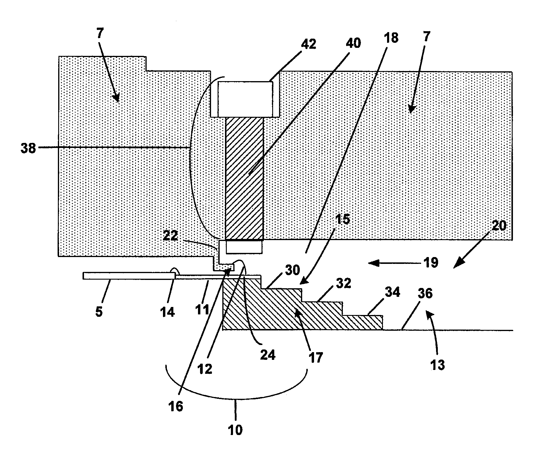
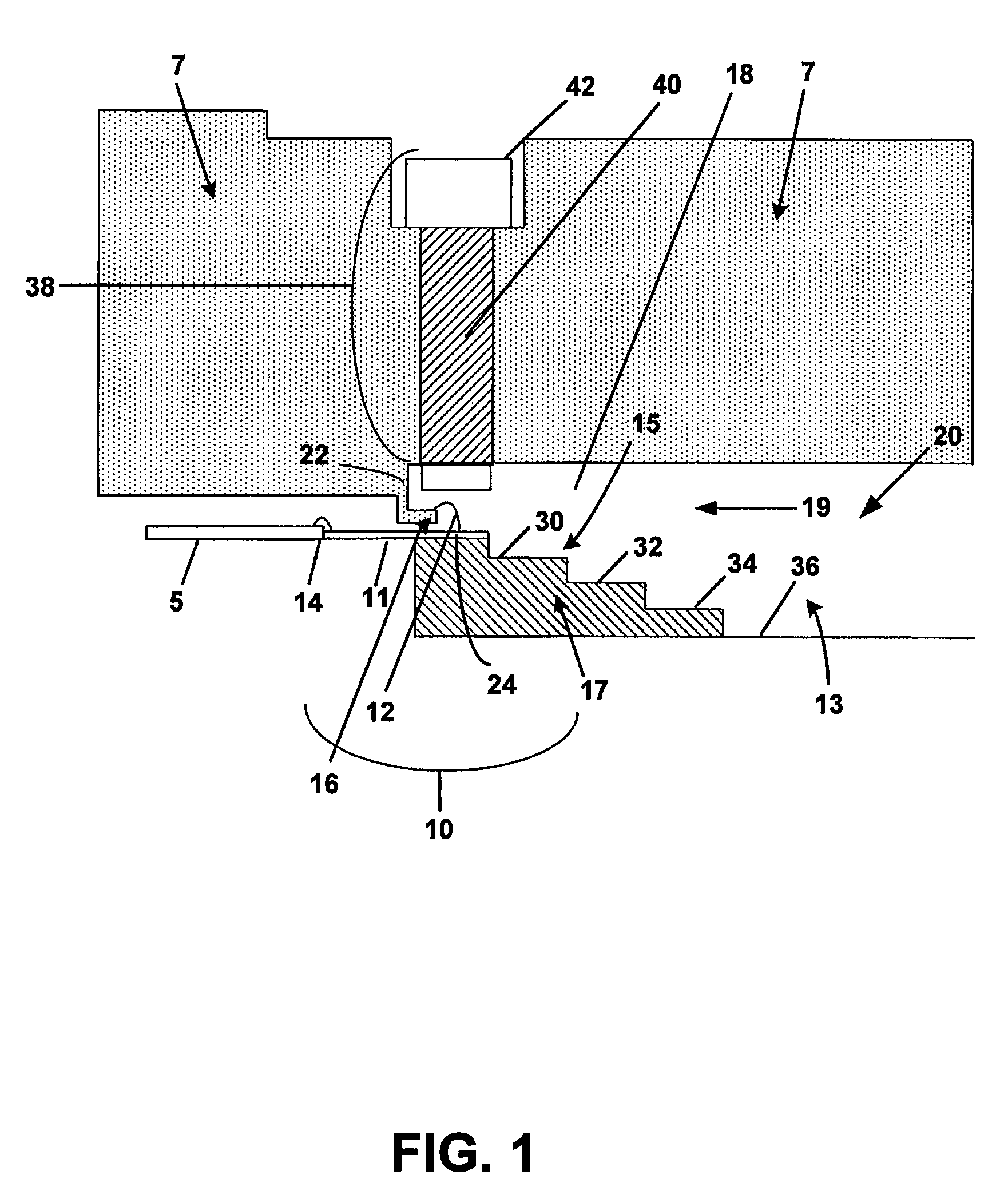
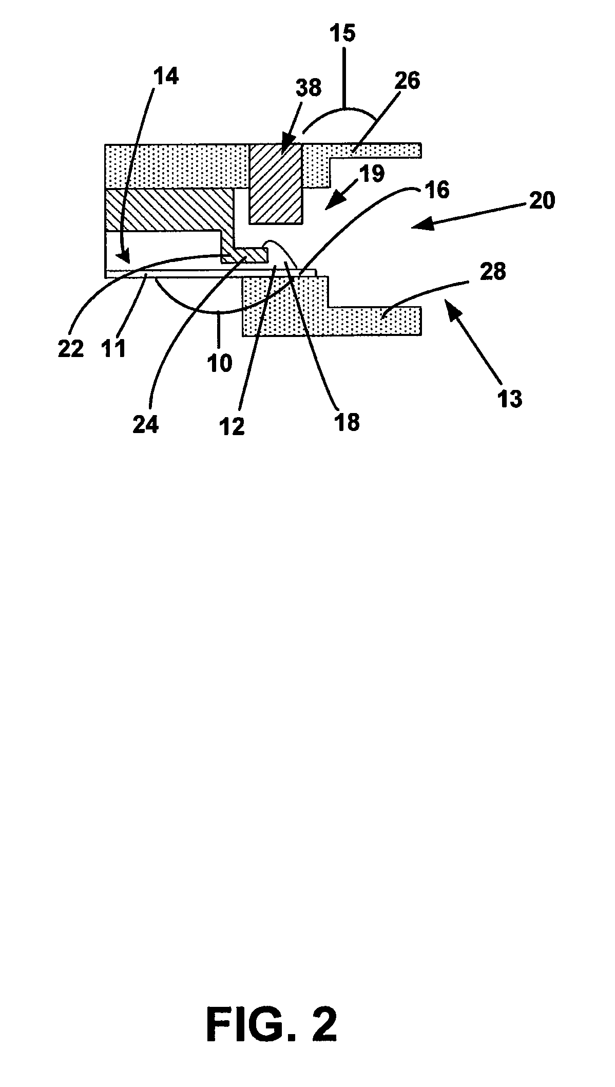
[0020]In accordance with one aspect of the present invention, an interface for connecting an integrated circuit to an energy transmission device such as a waveguide is disclosed. Throughout, the interface will be referred to as interface 10.

[0021]With reference to FIGS. 1-7, and in accordance with an exemplary embodiment of the present invention, an interface 10 is provided between an integrated circuit 11 and an energy transmission device 13. Certain exemplary interfaces 10 that may be used with the present invention are disclosed in co-pending and commonly owned U.S. patent application Ser. No. 11 / 853,287 entitled “Low-Loss Interface” which is incorporated in its entirety by reference.

[0022]Interface 10 connects integrated circuit 11, such as a MMIC, to another energy transmission device 13 such as a waveguide. While the terms integrated circuit 11 and energy transmission device 13 are used herein, it should be understood that interface 10 can connect any energy transmission, rece...


PUM


Abstract

In general, in accordance with an exemplary aspect of the present invention, a low-loss interface for connecting an integrated circuit such as a monolithic microwave integrated circuit to an energy transmission device such as a waveguide is disclosed. The interface comprises an isolation wall placed between an input and output region of an integrated circuit to reduce ripple and isolate the waveguide cavity from the monolithic microwave integrated circuit circuitry. The interface further comprises a turning screw or other similar member that is configured to closely match the impedance of integrated circuit 11 with the impedance at interface 10 to further reduce loss.

Description

FIELD OF INVENTION[0001]The present invention generally relates to an interface for use, for example, between an integrated circuit and a waveguide. More particularly, the present invention relates to an impedance matching interface such as a step launch that transports or transforms energy from an integrated circuit, such as a monolithic microwave integrated circuit. In one exemplary embodiment, the impedance matching capability is adjustable.BACKGROUND OF THE INVENTION[0002]There are numerous circuits and other electronic devices that produce energy waves, such as electromagnetic waves and microwaves. These circuits produce energy waves that are delivered to a destination through different wires, guides, and other mediums.[0003]Transitioning microwave signals from one mode to another or interfacing to another medium is “lossy.” By being lossy, a portion of the signal is lost as it travels through the circuits, wires, and other mediums. Stated another way, a signal entering a lossy...

Claims


Application Information

Patent Timeline
Patent Type & Authority Patents(United States)
IPC IPC(8): H01P5/107
CPCH01P5/107
Inventor WOODS, CHARLESLOPEZ, NOEL
Owner VIASAT INC
Why Eureka
Try Eureka