Package for a semiconductor light emitting device

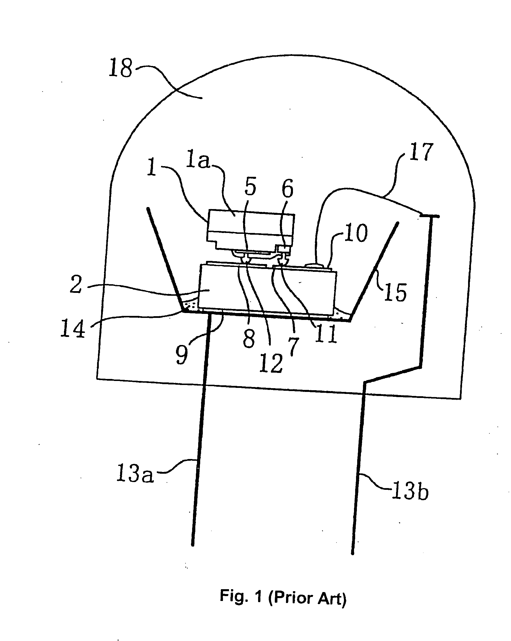
a light-emitting device and semiconductor technology, applied in semiconductor devices, solid-state devices, basic electric elements, etc., can solve the problems of heat generation, isolated device failure, and heat generation, and achieve the effect of efficient removal of heat and convenient mounting and connection of multiple chips

Inactive Publication Date: 2005-03-03
LUMILEDS
View PDF15 Cites 65 Cited by
  • Summary
  • Abstract
  • Description
  • Claims
  • Application Information

AI Technical Summary

Benefits of technology

[0010] The materials used in the package may be chosen to efficiently remove heat from the light emitting device, to have an insulating layer to facilitate mounting and connection of multiple chips, and to closely match the coefficient of thermal expansion (CTE) of the light emitting device and any intervening structure.

Problems solved by technology

The package of FIG. 1 does not efficiently conduct heat away from LED element 1.
In addition, some of the photons generated by radiative recombination are absorbed within the device, creating additional heat.
The inability of the package of FIG. 1 to conduct heat away from LED element 1 can lead to hot spots and isolated device failures.
In addition, the package of FIG. 1 does not easily allow for multiple devices, such as multiple LED elements or chips containing other circuitry, to be connected to lead frames 13a and 13b.
The problems with the package of FIG. 1 become severe design limitations as newer generations of LEDs are planned to be operated at higher power, for example, 1 W to 500 W, and in higher temperature environments, leading to an increase in operating temperatures and heat production.

Method used


Image

  • Package for a semiconductor light emitting device
  • Package for a semiconductor light emitting device
  • Package for a semiconductor light emitting device

Examples


Embodiment Construction

[0018] According to embodiments of the invention, a semiconductor light emitting device is mounted, directly or indirectly, on a substrate including a copper layer. The substrate may be chosen (1) to efficiently remove heat from the light emitting device, (2) to facilitate mounting and connection of multiple chips, and (3) to closely match the coefficient of thermal expansion (CTE) of the light emitting device and any intervening structure.

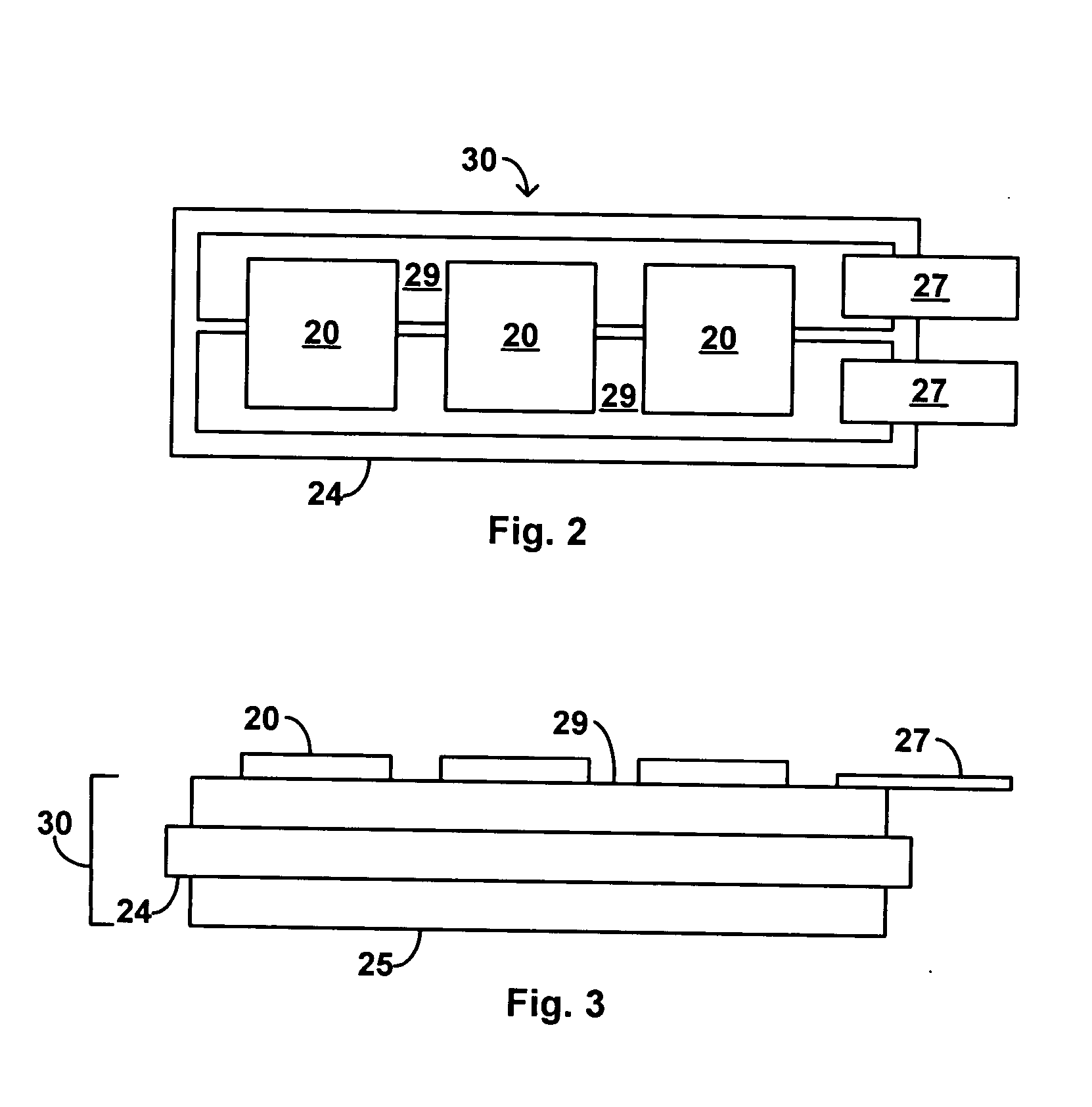
[0019]FIGS. 2 and 3 are a plan view and a cross sectional view of an embodiment of the invention. Semiconductor light emitting devices 20 are mounted on a substrate 30 including a thick copper layer (hereinafter referred to as a “copper substrate”).

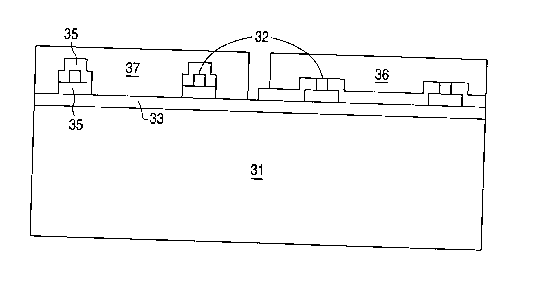
[0020] Copper substrate 30 includes an insulating core 24 and one or more thick regions of the metal 25 and 29. Core layer 24 and metal regions 25 and 29 are selected such that the composite of core layer 24 and metal regions 25 and 29 has a coefficient of thermal expansion matched to LED 20 and to ha...


PUM

PropertyMeasurementUnit
thicknessaaaaaaaaaa
thicknessaaaaaaaaaa
thermal conductivityaaaaaaaaaa

Abstract

A semiconductor light emitting device package includes a substrate with a core and a copper layer overlying the core. The light emitting device is connected to the substrate directly or indirectly through a wiring substrate. The core of the substrate may be, for example, ceramic, Al2O3, AlN, alumina, silicon nitride, or a printed circuit board. The copper layer may be bonded to the core by a process such as direct bonding of copper or active metal brazing.

Description

BACKGROUND [0001] 1. Field of Invention [0002] The present invention relates to a package for a semiconductor light emitting device and, in particular, to a package including a substrate with a thick copper layer. [0003] 2. Description of Related Art [0004] Semiconductor light emitting devices such as light emitting diodes (LEDs) are among the most efficient light sources currently available. Material systems currently of interest in the manufacture of high brightness LEDs capable of operation across the visible spectrum include group Ill-V semiconductors, particularly binary, ternary, and quaternary alloys of gallium, aluminum, indium, and nitrogen, also referred to as III-nitride materials; and binary, ternary, and quaternary alloys of gallium, aluminum, indium, and phosphorus, also referred to as III-phosphide materials. Often III-nitride devices are epitaxially grown on sapphire, silicon carbide, or III-nitride substrates and III-phosphide devices are epitaxially grown on galliu...

Claims


Application Information

Patent Timeline
Patent Type & Authority Applications(United States)
IPC IPC(8): H01L23/373H01L33/08H01L33/38H01L33/64H05K1/03
CPCH05K1/0306H01L2924/12041H01L2224/45144H01L33/08H01L33/38H01L2924/01322H01L33/647H01L2224/48091H01L2224/48247H01L2924/01079H01L2924/01019H01L33/64H01L2924/00014H01L2924/00C04B2237/407
Inventor WALL, FRANKLIN J. JR.
Owner LUMILEDS
Why Eureka
Try Eureka