Circuit package having low modulus, conformal mounting pads

a technology of conformal mounting and circuit package, which is applied in the direction of printed circuit stress/warp reduction, dielectric characteristics, electrical apparatus construction details, etc., can solve the problems of increasing the amount of heat which must be dissipated by the package, increasing the magnitude of temperature, and increasing the chip siz

Inactive Publication Date: 2002-06-04
IBM CORP
View PDF25 Cites 55 Cited by
  • Summary
  • Abstract
  • Description
  • Claims
  • Application Information

AI Technical Summary

Problems solved by technology

However, increased chip size also increases the dimensional change of the chip during thermal excursions.
Moreover, including more chips within a single package as well as increased functionality of each chip tends to increase the amount of heat which must be dissipated by the package.
This also increases the magnitude of temperature excursions and resultant dimensional changes of the chip and other structures in the package such as lead frames or laminated chip carriers for making mechanical and electrical connections to individual chips printed circuit boards for making connections between chips and to package terminals and connection structures between the chip carriers and the printed circuit board.
This stand-off distance appears to compromise the mechanical connection between the PCB and the chip.
Moreover, the high aspect ratio connections are substantially cantilevers which would be deflected during different relative accelerations of the chip and PCB, compromising reliability.
Alternative reinforced materials having intermediate CTEs which are more closely matched to the CTE of a chip are available such as S-glass, aramid, invar, LCP, etc. but are many times more expensive to purchase or process and prohibitive for most PCB production applications.
Bonded wire connections are known to be more compliant but are time consuming and expensive to fabricate, present additional failure modes and

Method used


Image

  • Circuit package having low modulus, conformal mounting pads
  • Circuit package having low modulus, conformal mounting pads
  • Circuit package having low modulus, conformal mounting pads

Examples


Embodiment Construction

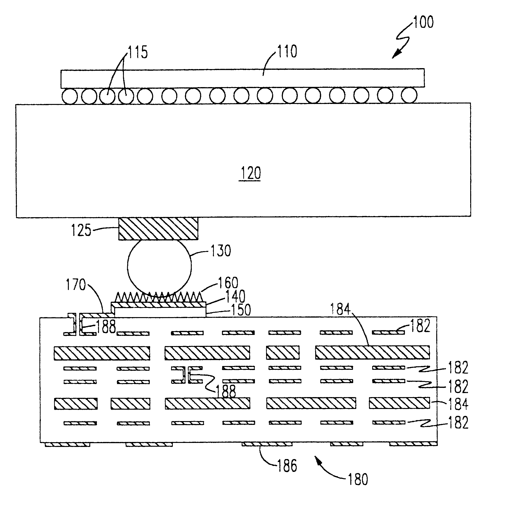
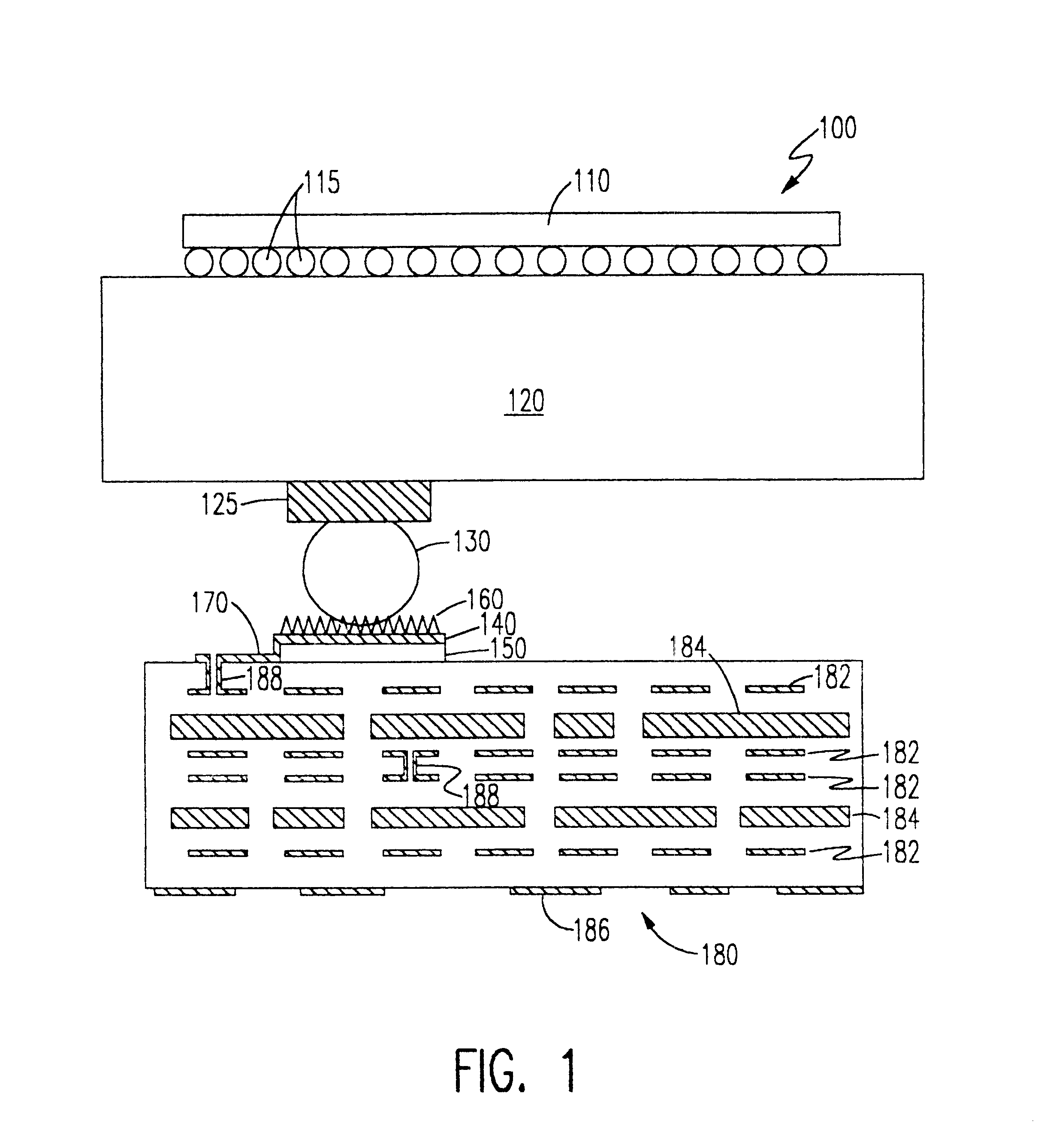
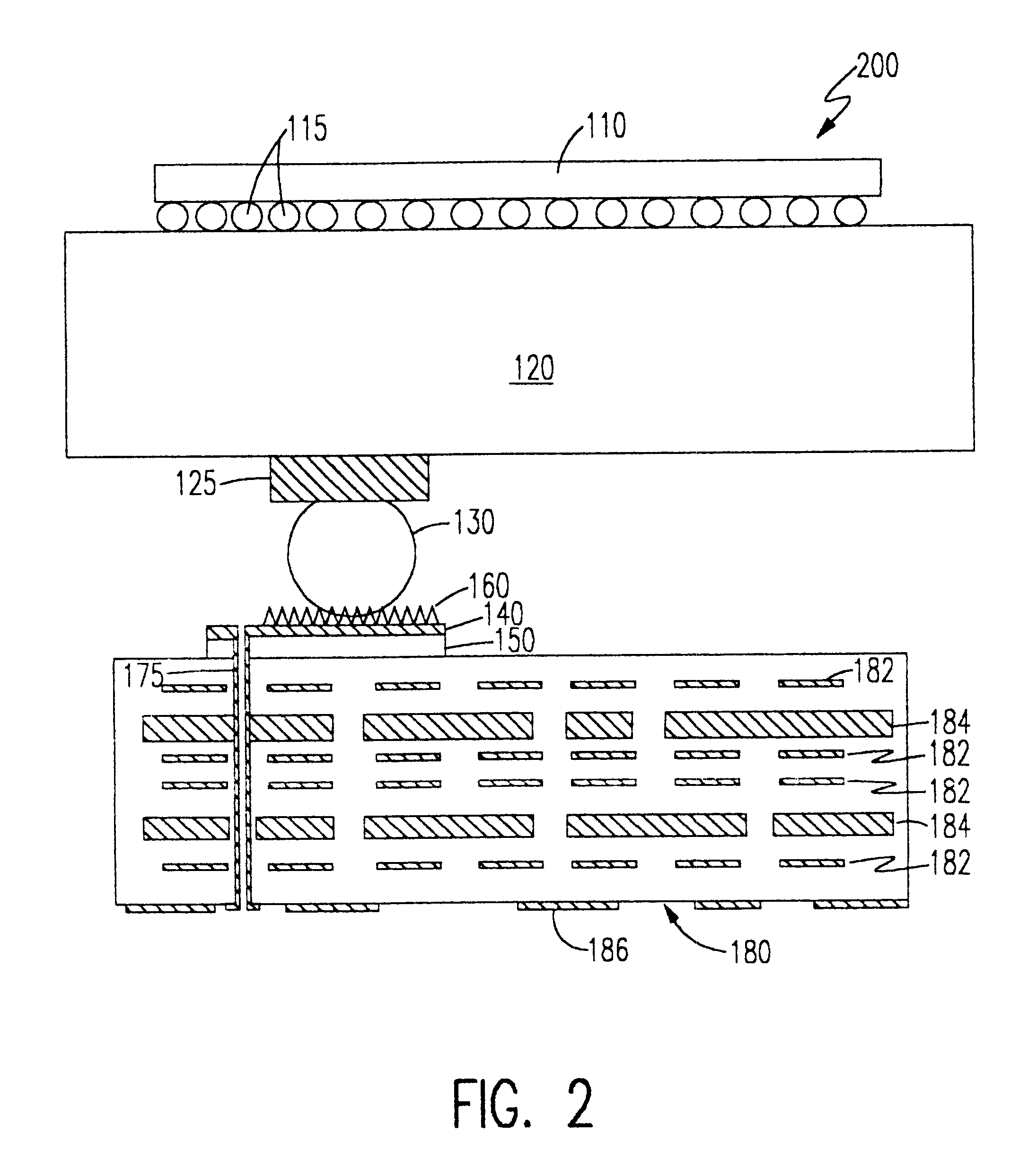
Referring now to the drawings, and more particularly to FIG. 1, there is shown, in cross- sectional view, a preferred embodiment 100 of the invention. The basic principle of the invention illustrated in FIG. 1 and other Figures is to place low modulus, dimensionally compliant materials only where necessary in relatively low aspect ratio (e.g. 1:1 or less in ratio of connection pad height to transverse dimension) deposits to avoid or reduce stressing of electrical connections, principally between the LCC and PCB, or the chip during thermal cycling of the package.

Specifically, in accordance with the invention, low modulus materials, preferably in the range of 1000 to 200,000 PSI, are used only directly under or as the mounting pad surface, preferably in the form of bumps or filled mounting wells in order to decouple stresses between packaging levels while largely avoiding compromise of heat transfer from the chip. The surface of low modulus material can be metallized, preferably with ...


PUM


Abstract

Reliability of circuit packaging while accommodating larger chips and increased temperature excursions is achieved by use of compliant pads only at the locations of connections between packaging levels, preferably between a laminated chip carrier and a printed circuit board. The invention allows the coefficient of thermal expansion of the chip carrier to be economically well-matched to the CTE of the chip and accommodation of significant differences in CTEs of package materials to be accommodated at a single packaging level. The compliant pads are preferably of low aspect ratio which are not significantly deflected by accelerations and can be formed on a surface or recessed into it. Connections can be made through surface connections and/or plated through holes. Connection enhancements such as solder wettable surfaces or dendritic textures are provided in a conductive metal or alloy layer over a compliant rubber or elastomer layer which may be conductive or non-conductive.

Description

1. Field of the InventionThe present invention generally relates to the packaging of integrated circuit chips and, more particularly, to package structures and materials for very large scale integrated circuits and packages including a plurality of such chips in which the reliability of connections is enhanced.2. Description of the Prior ArtThe advantages of very high integration density in regard to circuit performance and manufacturing economy have been recognized for some years. Connections of reduced length have reduced capacitance and resistance, reducing signal propagation time and power requirements while increasing noise immunity. Reduced signal propagation time and increased noise immunity can also be developed by minimizing the length of connections between chips, as well. Increased chip functionality can be obtained at lower manufacturing cost by forming more devices (e.g. transistors, storage cells and the like) on a single wafer. For these reasons, there is a trend towa...

Claims


Application Information

Patent Timeline
IPC IPC(8): H05K3/32H05K1/02H05K1/11
CPCH05K1/0271H05K3/326H05K1/111H05K1/114H05K2203/0307H05K2201/0133H05K2201/0187H05K2201/10734
Inventor DOWNES, JR., FRANK J.FARQUHAR, DONALD S.JAPP, ROBERT M.RUDIK, WILLIAM J.
Owner IBM CORP
Why Eureka
Try Eureka