Wire loop, semiconductor device having same and wire bonding method

a technology of wire loop and semiconductor device, which is applied in the direction of auxillary welding device, semiconductor/solid-state device details, soldering apparatus, etc., can solve the problems of unstable neck portion h, prone to damage, and high wire loop height, and achieve low profile and stably bent

Active Publication Date: 2010-10-19
KAIJOO KK
View PDF18 Cites 34 Cited by
  • Summary
  • Abstract
  • Description
  • Claims
  • Application Information

AI Technical Summary

Benefits of technology

[0015]Accordingly, it is an object of the present invention to provide a wire loop having a low profile which is stable and of which a neck portion is hard to damage while no crushed part is formed by a capillary on a wire and a ball bonded to a first bonding point.
[0034]According to the present invention, the wire loop is provided on the neck portion thereof with the inclined riser part which is formed by a top portion of the ball which has entered an opening of a capillary and been shaped at the time of ball bonding, so that the wire loop has a low profile which is stable and which is formed without any damage caused to a neck portion thereof. In the preferred embodiment of the invention, the wire of the entire wire loop can be stably bent by forming a plurality of bends at desired locations of the wire by the capillary being moved obliquely upward or by the capillary being moved upward and then horizontally or by the capillary being moved upward and then obliquely downward.

Problems solved by technology

However, in the above-described techniques, as the wire loop includes the neck portion H having a somewhat large height, the wire loop becomes high and thus is rendered unstable.
In addition, in a case where a wire loop is formed without any reverse operation of the capillary in order to make the height of a neck portion H thereof small and the height of the neck portion H is reduced to a certain level or below, the neck portion H is liable to be damaged in drawing or moving the wire 3 to arrange it in place because of the wire 3 vertically extending from the first bonding point A.
However, in the technique disclosed in U.S. Patent Application Publication No. 2004 / 0104477, since part of the wire and the top of the bonded ball is crushed by the capillary at the first bonding point, there is a possibility that the first bonding point will be damaged.

Method used


Image

  • Wire loop, semiconductor device having same and wire bonding method
  • Wire loop, semiconductor device having same and wire bonding method
  • Wire loop, semiconductor device having same and wire bonding method

Examples


Embodiment Construction

[0051]Now, a wire loop, a semiconductor device and a wire bonding method according to the present invention will be described hereinafter with reference to the accompanying drawings in which like parts in each of the several figures are identified by the same reference character or numeral.

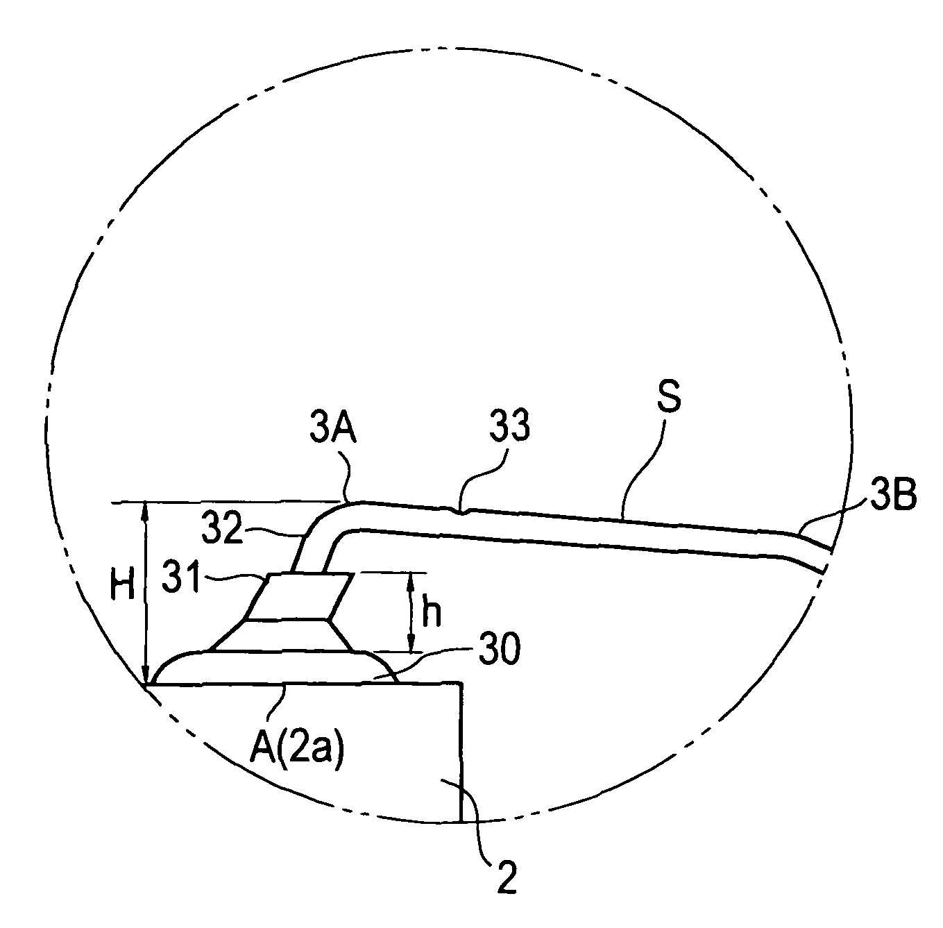
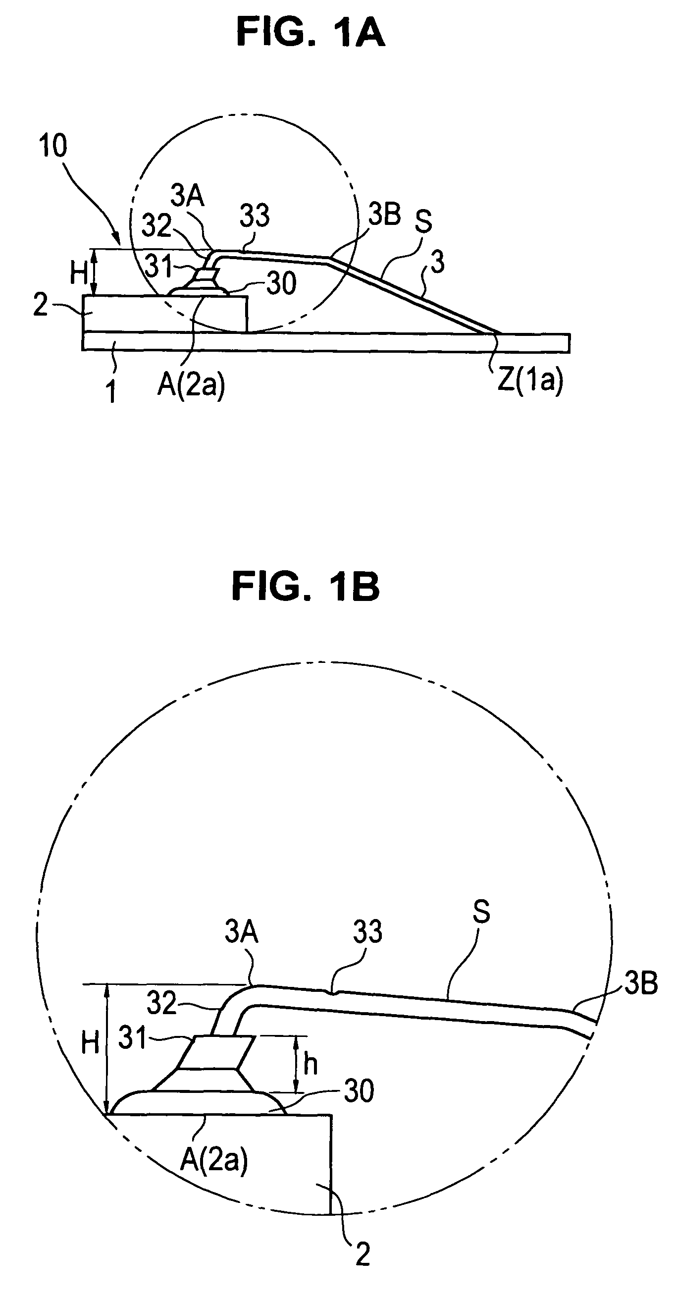
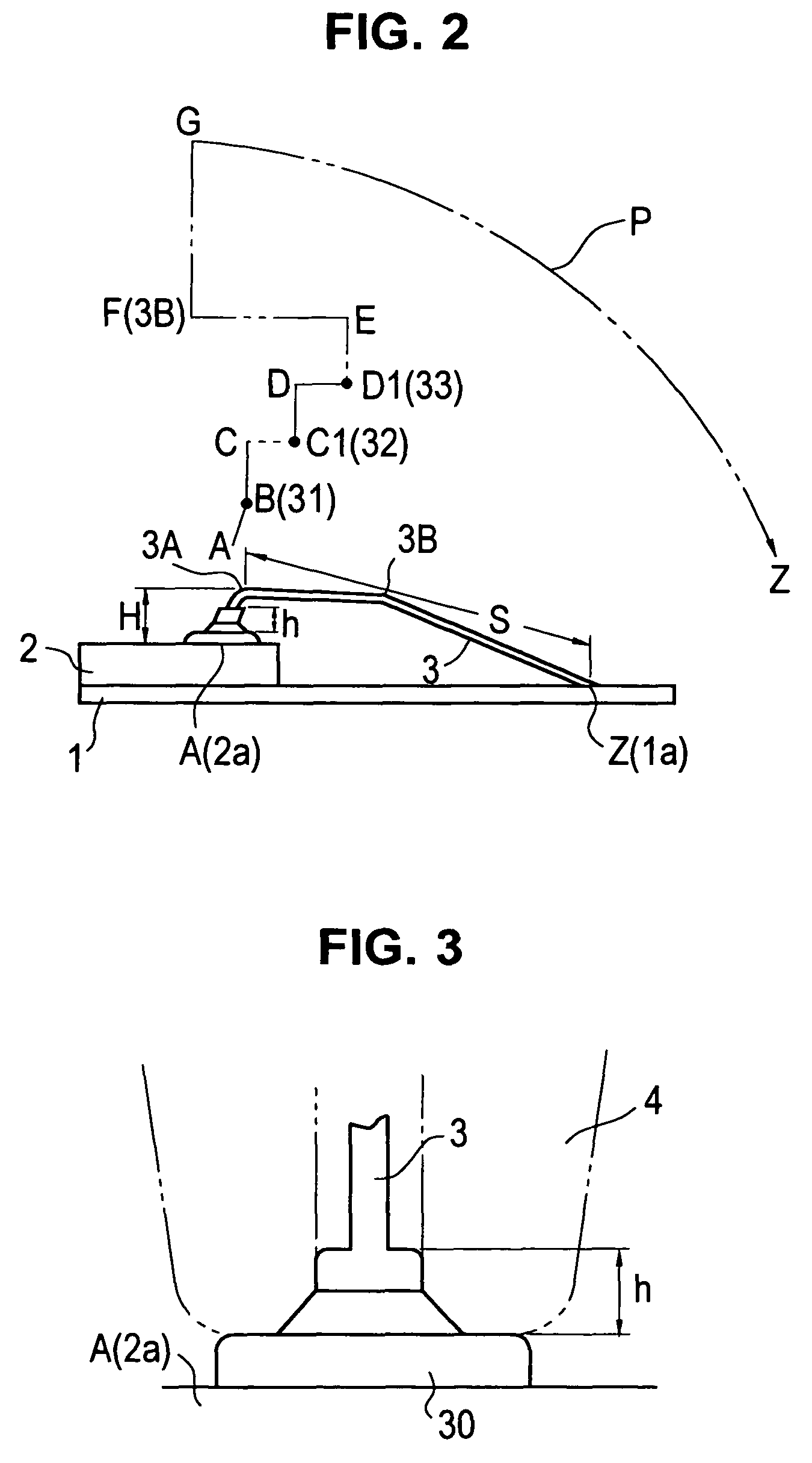
[0052]Referring first to FIGS. 1A and 1B, an embodiment of a wire loop and a semiconductor device 10 having the wire loop incorporated therein according to the present invention is illustrated. In the semiconductor device 10, a semiconductor chip 2 is attached to a lead frame 1 and is provided thereon with a pad 2a which is a first bonding point A. The wire loop of a wire 3 is formed to have a substantially triangular shape in general and includes a neck portion H having a ball 30 bonded to the pad 2a or first bonding point A and a major portion or generally inclined portion S which has an end bonded to a lead la of the lead frame 1 or a second bonding point Z. The neck portion H and the major por...


PUM

PropertyMeasurementUnit
maximum vertical heightaaaaaaaaaa
heightaaaaaaaaaa
heightaaaaaaaaaa

Abstract

A wire loop comprises a wire connecting a first bonding point and a second bonding point therethrough, wherein the wire includes a ball bonded to the first bonding point, a neck portion adjacent to the ball and a major portion extending from the neck portion to the second bonding point. The neck portion includes a riser part which extends, from the bonded ball, obliquely upward in a direction toward the second bonding point, and the riser part is formed by a top portion of the ball which has entered an opening of a capillary and been shaped at the time of ball bonding. The riser part is formed by inclining the top portion of the ball, which enters the opening of the capillary at the time of ball bonding, which inclining is done by moving the capillary obliquely upward toward the second bonding point.

Description

BACKGROUND OF THE INVENTION[0001]1. Field of the Invention[0002]The present invention relates to a wire bonding method for connecting a first bonding point and a second bonding point through a wire, a wire loop having a certain shape and a semiconductor device having such a wire loop incorporated therein.[0003]2. Description of the Related Art[0004]Conventionally, in a process of fabricating a semiconductor device, as shown in FIG. 9A or 9B, wire bonding for connecting a pad 2a or a first bonding point A of a semiconductor chip 2 attached to a lead frame 1 and a lead 1a or a second bonding point Z of the lead frame 1 through a wire 3 has been carried out. Typically, loop shapes of the wire 3 connecting the first and second bonding points A and Z include a trapezoidal shape and a triangular shape shown in FIGS. 9A and 9B, respectively, as disclosed, for example, in U.S. Pat. No. 6,036,080 or Japanese Patent Application Laid-Open Publication No. 2000-277558.[0005]The wire loop having ...

Claims


Application Information

Patent Timeline
Patent Type & Authority Patents(United States)
IPC IPC(8): B23K31/00
CPCH01L2924/00H01L2224/8518H01L24/48H01L2924/01006H01L24/85B23K2201/32H01L2924/01033H01L2924/01082H01L2224/85181H01L2924/01057H01L2224/05599H01L2224/45099H01L2924/01004H01L2224/48227H01L2224/48091H01L2924/00014H01L2224/48465H01L2224/85148H01L2224/85399H01L2224/48095B23K20/004H01L2924/01005H01L24/78H01L2224/78301H01L2924/01015H01L2924/01002B23K2101/32H01L2224/85205H01L2924/181H01L23/488
Inventor FUJISAWA, HIROMIISHIBASHI, MASARUIMAI, REI
Owner KAIJOO KK
Why Eureka
Try Eureka