Organic thin-film transistor

a thin-film transistor and organic technology, applied in the direction of discharge tube luminescnet screens, thermoelectric devices, natural mineral layered products, etc., can solve the problems of low heat resistance and inability to form organic thin-film transistors on plastic boards with low heat resistance, and achieve the effect of high transportability

Inactive Publication Date: 2010-10-19
RICOH KK
View PDF11 Cites 27 Cited by
  • Summary
  • Abstract
  • Description
  • Claims
  • Application Information

AI Technical Summary

Benefits of technology

[0008]In an aspect of this disclosure, there is provided an organic thin-film transistor having high transportability, which can be prepared by applying simple processes, such as coating and printing.

Problems solved by technology

Therefore, the organic thin-film transistors can be formed on a plastic board typically having low heat resistance.
Therefore, this is not as simple as the methods such as printing method and spin coat method mentioned above.

Method used


Image

  • Organic thin-film transistor
  • Organic thin-film transistor
  • Organic thin-film transistor

Examples


example 1

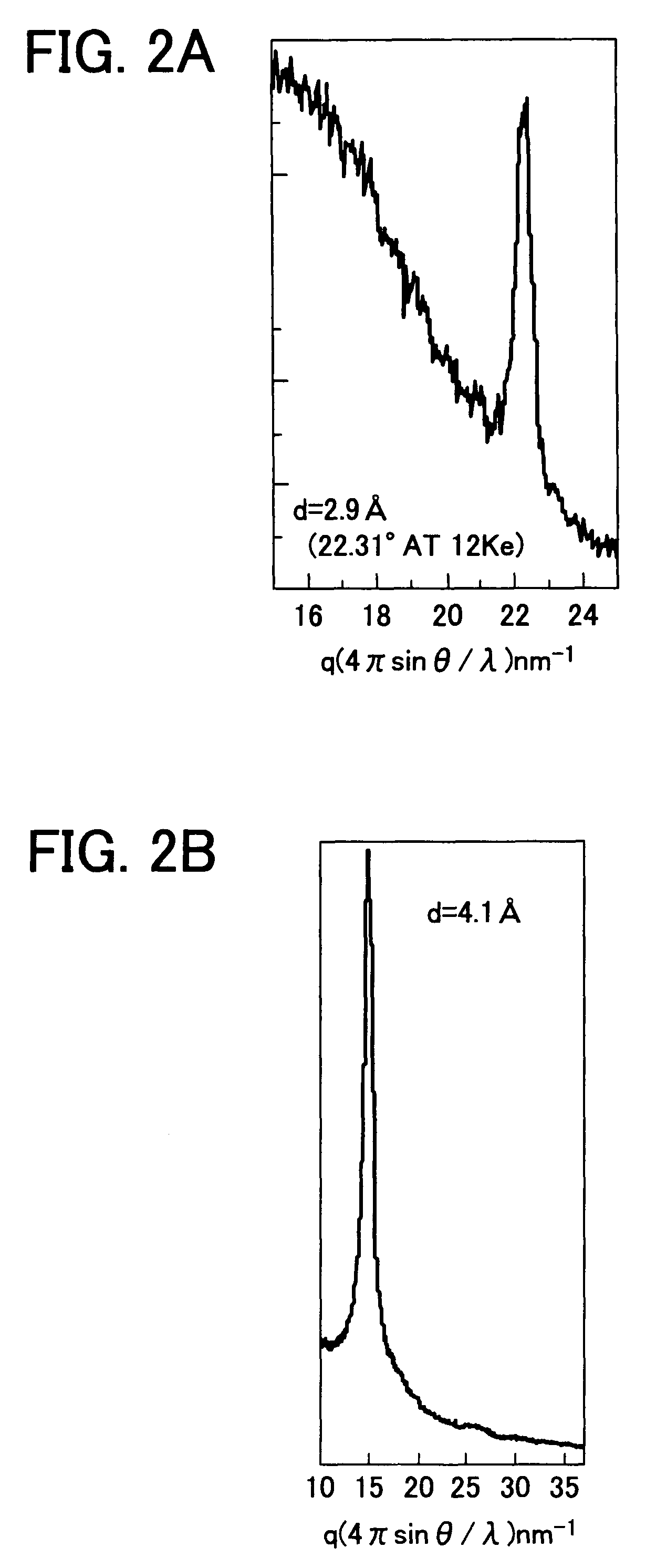
[0052]The substrate for organic thin-film transistor prepared as above was dipped in a toluene solution including phenyltrichlorosilane in an amount of 5 mM for 30 min while exposed with ultrasonic, and dried. The structural analysis of the thus treated substrate is shown in FIG. 2A. A structure having a surface separation of 2.9 Å and a half width not greater than ±0.1 Å can be identified.

[0053]In FIGS. 2A and 2B, when the X-ray diffraction is measured, 2θ is typically used for a horizontal axis. When 2θ is a surface separation (d) and a measurement wavelength (λ), a diffraction peak appears at a point where 2d sin θ=λ. When the measurement wavelength (λ) and the diffraction angle θ are fixed, the surface separation d is identified. Cukα ray having λ of known 1.1418 Å is typically used for the measurement, and 2θ can be used.

[0054]However, in terms of balance between a sample damage (low energy damages an organic material) and a measurement range (high energy causes a low angle, re...

example 2

[0065]The procedure for preparation of the organic thin-film transistors in Example 1 was repeated to prepare two organic thin-film transistors except for mixing an organic semiconductive compound having the following formula

[0066]

with the organic semiconductive compound in Example 1 such that the organic semiconductive compounds had a mixing ratio (Example 1 / Example 2) of 6 / 4.

[0067]The field-effect transportabilities of the organic thin-film transistors were 4.1×10⁻³ cm2 / Vs, respectively as shown in FIG. 4.

[0068]The organic thin-film transistors had no variations between the elements and good reproducibilities.

example 3

[0069]The procedure for preparation of the organic thin-film transistors in Example 1 was repeated to prepare two organic thin-film transistors except that the substrate was dipped in a toluene solution including phenethyltrichlorosilane in an amount of 5 mM for 30 min while exposed with ultrasonic, and dried. The field-effect transportabilities of the organic thin-film transistors were 2.8×10⁻³ cm2 / Vs, respectively as shown in FIG. 5.


PUM

PropertyMeasurementUnit
thicknessaaaaaaaaaa
thicknessaaaaaaaaaa
incident energyaaaaaaaaaa

Abstract

An organic thin-film transistor, including a layer exposing a benzene ring, having a surface separation of from 2.8 to 3.0 Å; and an organic semiconductive layer located overlying the layer exposing a benzene ring.

Description

BACKGROUND[0001]1. Technical Field[0002]This disclosure relates to an organic thin-film transistor having an organic semiconductive layer.[0003]2. Discussion of the Related Art[0004]Recently, research and development of organic thin-film transistors using organic semiconductive materials has become popular. Thin films of the organic semiconductive materials can easily be formed simple wet process methods such as printing method and spin coat method. Compared with conventional thin-film transistors using inorganic semiconductive materials, it is advantageous that the organic thin-film transistors can be prepared at a low temperature. Therefore, the organic thin-film transistors can be formed on a plastic board typically having low heat resistance. Then, the weight and cost of electronics devices such as a display can be saved and various applications such as applications taking advantage of the flexibility of the plastic board can be expected.[0005]Japanese Published Unexamined Paten...

Claims


Application Information

Patent Timeline
Patent Type & Authority Patents(United States)
IPC IPC(8): H01L29/08
CPCH01L51/0533H01L51/0059H01L51/0038H01L51/0035H01L51/0545H01L51/0043H10K85/111H10K85/114H10K85/151H10K85/631H10K10/476H10K10/466H10K10/484
Inventor KATO, TAKUJIARUGA, TAMOTSUGOTO, DAISUKETORII, MASAFUMIMATSUMOTO, SHINJI
Owner RICOH KK
Why Eureka
Try Eureka