
Semiconductor memory device with low standby current

a memory device and low standby current technology, applied in the field of semiconductor memory devices, can solve the problem that the standby current has not been sufficiently reduced in the conventional sram

Active Publication Date: 2010-11-02
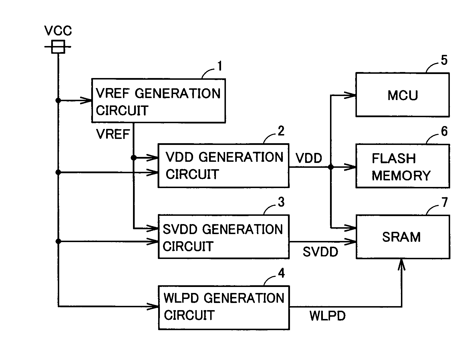
RENESAS ELECTRONICS CORP
View PDF6 Cites 14 Cited by
  • Summary
  • Abstract
  • Description
  • Claims
  • Application Information

AI Technical Summary

Benefits of technology

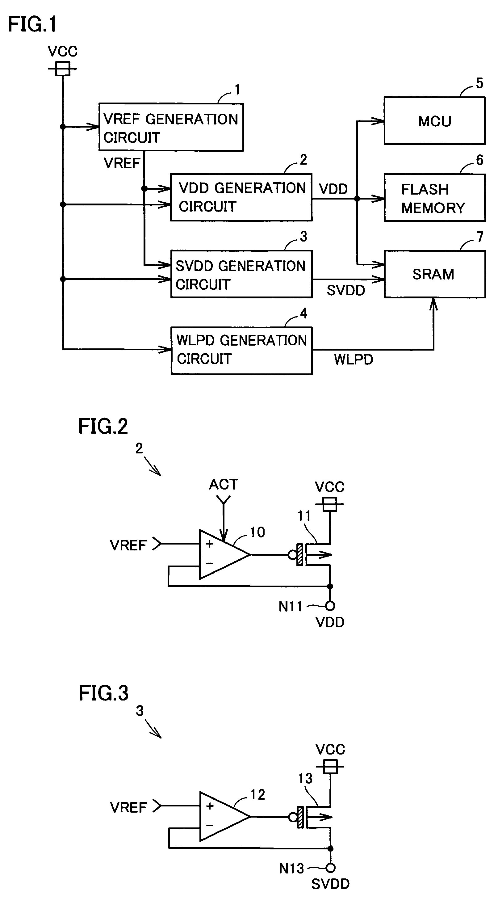
The present invention provides a semiconductor memory device with a low standby current. This is achieved by including a memory cell and a write / read circuit in the semiconductor memory device. The write / read circuit is driven by a second power supply voltage during a normal operation and its P-channel MOS transistor has a back gate receiving the first power supply voltage. When the second power supply voltage is shut off during standby, a pull-up circuit provides the first power supply voltage to the gate of the P-channel MOS transistor to bring it out of conduction, resulting in only a small amount of standby current. The second P-channel MOS transistor has a higher second threshold voltage than the first P-channel MOS transistor, which further reduces the standby current.

Problems solved by technology

However, a standby current has not sufficiently been reduced in the conventional SRAM.

Method used


Image

  • Semiconductor memory device with low standby current
  • Semiconductor memory device with low standby current
  • Semiconductor memory device with low standby current

Examples


second embodiment

[0063]FIG. 9 is a circuit block diagram that shows a substantial part of an SRAM according to a second embodiment of the present invention, in comparison with FIG. 6. With reference to FIG. 9, the SRAM differs from the SRAM in the first embodiment in that transistors 50-56 are replaced with transistors 70-76, respectively, and that internal power supply voltage VDD for a peripheral circuit is applied to each back gate of transistors 70-72, 75, 76. An absolute value of a threshold voltage of all the transistors 31-36, 50-56, 61-65 in FIG. 6 is 0.3 V, while an absolute value of a threshold voltage of transistors 70-76 is set to 0.5 V.

[0064]In the second embodiment, the threshold voltage of transistors 70-76 is set at a high level, and hence even if internal power supply voltage VDD is set to 0 V during standby, leakage current IL is small.

third embodiment

[0065]FIG. 10 is a circuit block diagram that shows a substantial part of an SRAM according to a third embodiment of the present invention, in comparison with FIG. 6. With reference to FIG. 10, the SRAM differs from the SRAM in the first embodiment in that internal power supply voltage VDD is applied to each back gate of P-channel MOS transistors 50-52, 55, 56, and that pull-up circuits (PU) 80-83 are added. Pull-up circuits 80-82 are connected to gates of P-channel MOS transistors 50-52, respectively, and pull-up circuit 83 is connected to gates of P-channel MOS transistors 55, 56. Each of pull-up circuits 80-83 pulls up the gate of the corresponding P-channel MOS transistor to an “H” level (internal power supply voltage SVDD) during standby, and fixes the corresponding P-channel MOS transistor to a non-conduction state.

[0066]As shown in FIG. 11, pull-up circuit 80 includes P-channel MOS transistors 84, 85 and an N-channel MOS transistor 86. P-channel MOS transistor 84 has a source...


PUM


Abstract

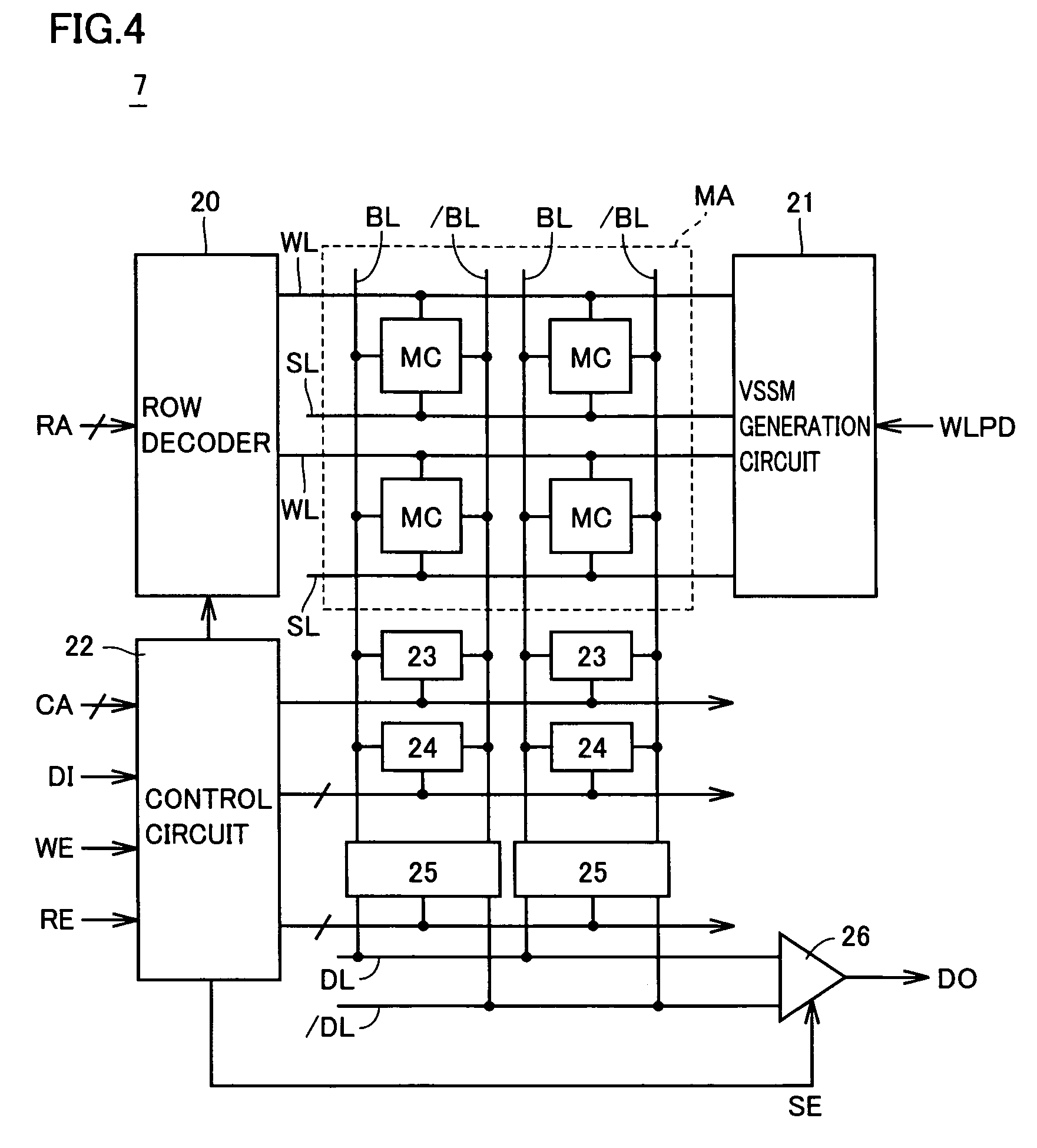
In an SRAM according to the present invention, an internal power supply voltage for a memory cell is applied to a back gate of each of P-channel MOS transistors included in an equalizer, a write driver, and a column select gate. Therefore, even if an internal power supply voltage for a peripheral circuit is shut off to reduce current consumption during standby, a threshold voltage of each of the P-channel MOS transistors is maintained at a high level, and hence a leakage current is small.

Description

BACKGROUND OF THE INVENTION[0001]1. Field of the Invention[0002]The present invention relates to a semiconductor memory device, and particularly relates to a semiconductor memory device in which a memory cell and a write / read circuit are driven by different power supply voltages, and in which the power supply voltage for the write / read circuit is shut off during standby to reduce a standby current.[0003]2. Description of the Background Art[0004]Conventionally, a reduction in standby current has been promoted in an SRAM (Static Random Access Memory). In some SRAMs, a power supply voltage SVDD for a memory cell and a power supply voltage VDD for a peripheral circuit are separately supplied, and power supply voltage VDD for the peripheral circuit is shut off during standby to reduce a standby current. Note that power supply voltage SVDD for the memory cell is not shut off even during standby for retaining stored data.[0005]Furthermore, in other SRAMs, a source voltage of a driver trans...

Claims


Application Information

Patent Timeline
Patent Type & Authority Patents(United States)
IPC IPC(8): G11C7/00
CPCG11C5/147G11C11/412
Inventor NAKAI, HIROAKISATO, HIROTOSHIAKAI, KIYOYASU
Owner RENESAS ELECTRONICS CORP
Learn More