Integrated capacitor for wafer level packaging applications

Inactive Publication Date: 2006-11-16
EKUBIK CONSULTING
View PDF1 Cites 14 Cited by
  • Summary
  • Abstract
  • Description
  • Claims
  • Application Information

AI Technical Summary

Benefits of technology

[0013] In another embodiment, the integrated capacitor structure can be used in a power storage unit for the power supply used in global positioning systems or other handheld devices. This design would minimize the overall number of capacitors in handheld devices and reduce the device form factor (x, y, z dimensions of the unit).
[0014] Thus, the integrated capacitor design provides a high capacitance material set for capacitor applications and is conducive to active integration in the substrate or electronic package. In one aspect, the integrated capacitor can be designed for high capacitance greater than or equal to 1 microfarad. The integrated capacitor design provides an integrated power delivery solution for electronic devices by incorporating a planar capacitor as an integral part of the substrate or die/wafer design. This design address

Problems solved by technology

Hence, the prior art design provides for an inefficient power delivery mechanism, to the die, due to a fairly large physical separation between the capacitor 10 and the die 16.
Furthermore, this design also degrades the structural integrity of the electronic package since the capacitor 10 is a discrete component that is sol

Method used


Image

  • Integrated capacitor for wafer level packaging applications
  • Integrated capacitor for wafer level packaging applications
  • Integrated capacitor for wafer level packaging applications

Examples


Embodiment Construction

[0035] Reference will now be made in detail to exemplary embodiments which are illustrated in the accompanying drawings (FIGS. 2-20).

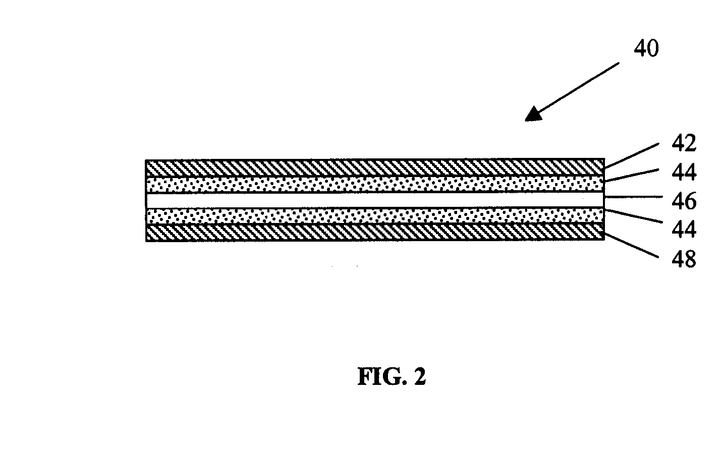
[0036] The integrated planar capacitor 40, as shown in FIG. 2, is formed as part of the substrate fabrication process. The capacitor 40 uses copper as the first electrode 42 which is also the rigid core base for the thin film substrate. Barium Strontium Titanate (BST), Lead Zirconate Titanate (PZT), Tantalum Oxide or other materials used in capacitor design and manufacturing and can be applied using Chemical Vapor Deposition (CVD), spin on or other coating type of techniques. A material such as mesoporous nanocomposite material 44, or other materials that promote adhesion are often applied to the copper to ensure adhesion of the high K dielectric to the copper. The mesoporous nanocomposite material 44 may be doped with a high K dielectric material 46 to further enhance the overall capacitance value. The second electrode is copper 48 which can be patte...


PUM


Abstract

A capacitor design, which incorporates a material set that is adaptable to standard substrate or electronic packaging fabrication methods, uses copper as a base and electrode, mesoporous nanocomposite materials or other adhesion promoting materials combined with a high dielectric material specific to the application's capacitance requirements. This capacitor is then used as a basis for forming a capacitor in substrate or package or wafer level package or die or wafer.

Description

RELATED APPLICATIONS [0001] This application is a Divisional of prior application Ser. No. 10 / 752,045, filed Jan. 5, 2004, entitled “System and Method for Packaging Electronic Components,” currently pending, herein incorporated by reference in its entirety.BACKGROUND [0002] 1. Field of the Invention [0003] The present invention relates to packaging electronic components for providing improved power delivery, enhanced structural integrity, and reduction in the dimensions of the packaging. [0004] 2. General Background [0005] The design goal for electronic devices, where decoupling and power dampening applications are required, is to reduce signal and power noise and / or reduce power overshoot and droop by placing a capacitor as close to the die as possible. Also, the longer the path from the die to an electronic component, such as a capacitor, the more capacitance is needed due to the increased inductance. [0006] The current state of the art is to place the electronic components, such ...

Claims


Application Information

Patent Timeline
IPC IPC(8): H01L21/00
CPCH01L23/49816H01L23/49822H01L23/5223H01L2224/16H01L2924/01029H01L2924/01078H01L2924/01019H01L2924/1517H01L2924/15311H01L2924/15312H01L2924/19041H01L2924/19105H01L2924/19106H01L2924/15153
Inventor VRTIS, JOAN K.
Owner EKUBIK CONSULTING
Why Eureka
Try Eureka