
Electrooptic apparatus substrate and examining method therefor and electrooptic apparatus and electronic equipment

a technology of electrooptic apparatus and substrate, which is applied in the direction of instruments, measurement devices, computing, etc., can solve the problems of increasing the time taken for feeding back the method of examining a finished product is not preferable from the viewpoint of management of manufacturing steps, and the delay in the detection of a poor product. , to achieve the effect of satisfying the measurement accuracy

Inactive Publication Date: 2010-11-23
SEIKO EPSON CORP
View PDF29 Cites 2 Cited by
  • Summary
  • Abstract
  • Description
  • Claims
  • Application Information

AI Technical Summary

Benefits of technology

The present invention provides an electrooptic apparatus substrate and examination method that can detect poor points, such as lacking pixels, without requiring a probe to be in contact with the outside. This is achieved by including multiple scan lines and multiple signal lines intersecting each other, multiple pixels disposed in a matrix in accordance with the intersections of the multiple scan lines and the multiple signal lines, and an amplifying unit electrically connected to the signal lines, to which a signal input to the pixels is input through the signal lines, for amplifying the potential of the input signal. The electrooptic apparatus substrate and examination method of the present invention allow for satisfactory measuring accuracy without contact of a probe from the outside and can improve production efficiency and reduce development periods and costs.

Problems solved by technology

However, the method of examining a finished product is not preferable from the viewpoint of management of manufacturing steps.
This is because the detection of a poor product is delayed since the poor product is detected after the steps of manufacturing the substrate.
This increases the time taken for feeding back the detection of a poor product to the step management.
As a result, the period with a low yield increases, which also increases the manufacturing cost.
Also in prototyping, in since the period from the evaluation of a prototype to the feedback to the design process increases, which may increase the development period and the development costs.
Furthermore, the repair of a poor point is difficult after the product is finished.
Accordingly, a poor point, especially, a lacking pixel in a display device is desirably detected within steps of manufacturing the substrate.

Method used


Image

  • Electrooptic apparatus substrate and examining method therefor and electrooptic apparatus and electronic equipment
  • Electrooptic apparatus substrate and examining method therefor and electrooptic apparatus and electronic equipment
  • Electrooptic apparatus substrate and examining method therefor and electrooptic apparatus and electronic equipment

Examples


first embodiment

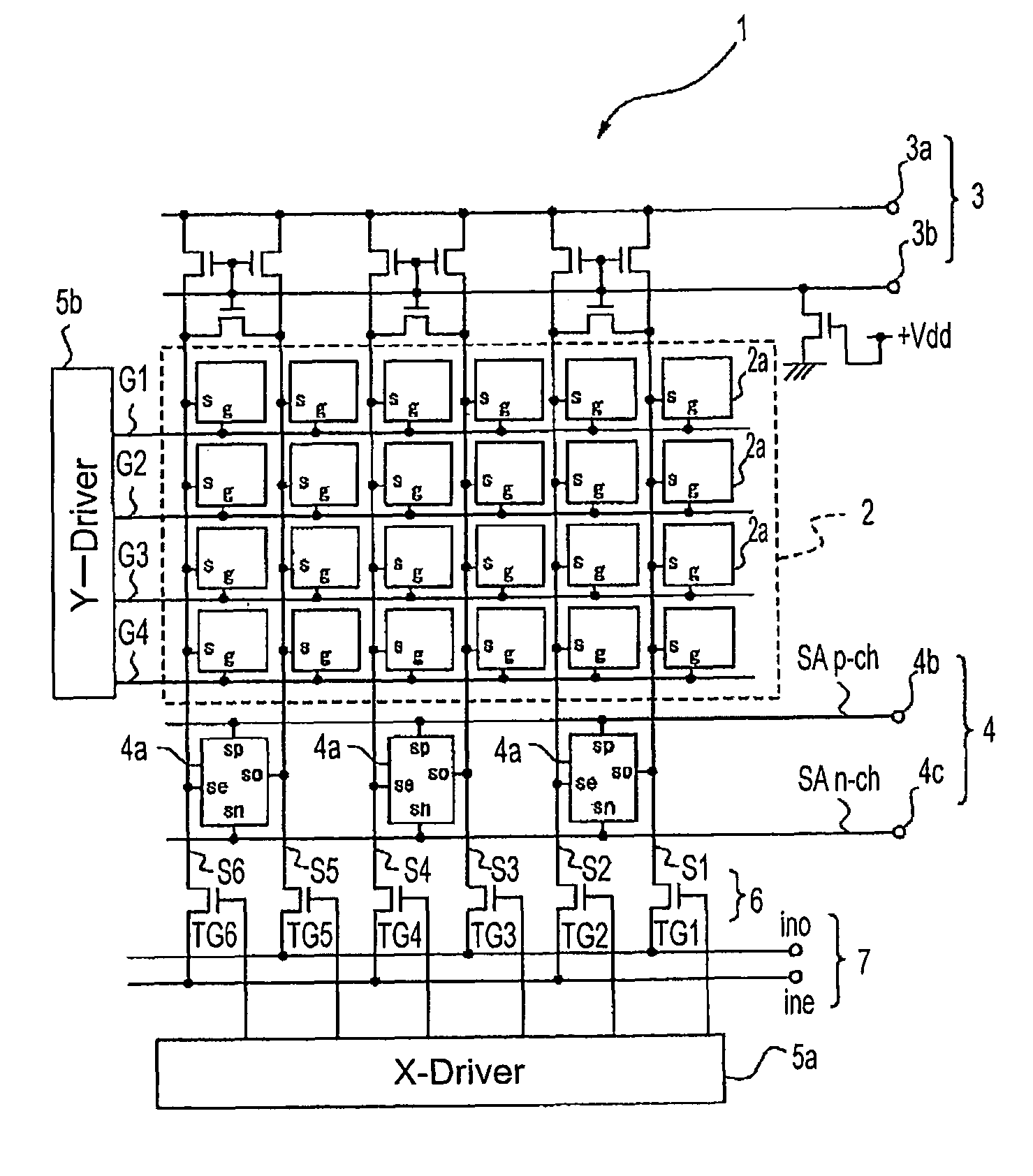
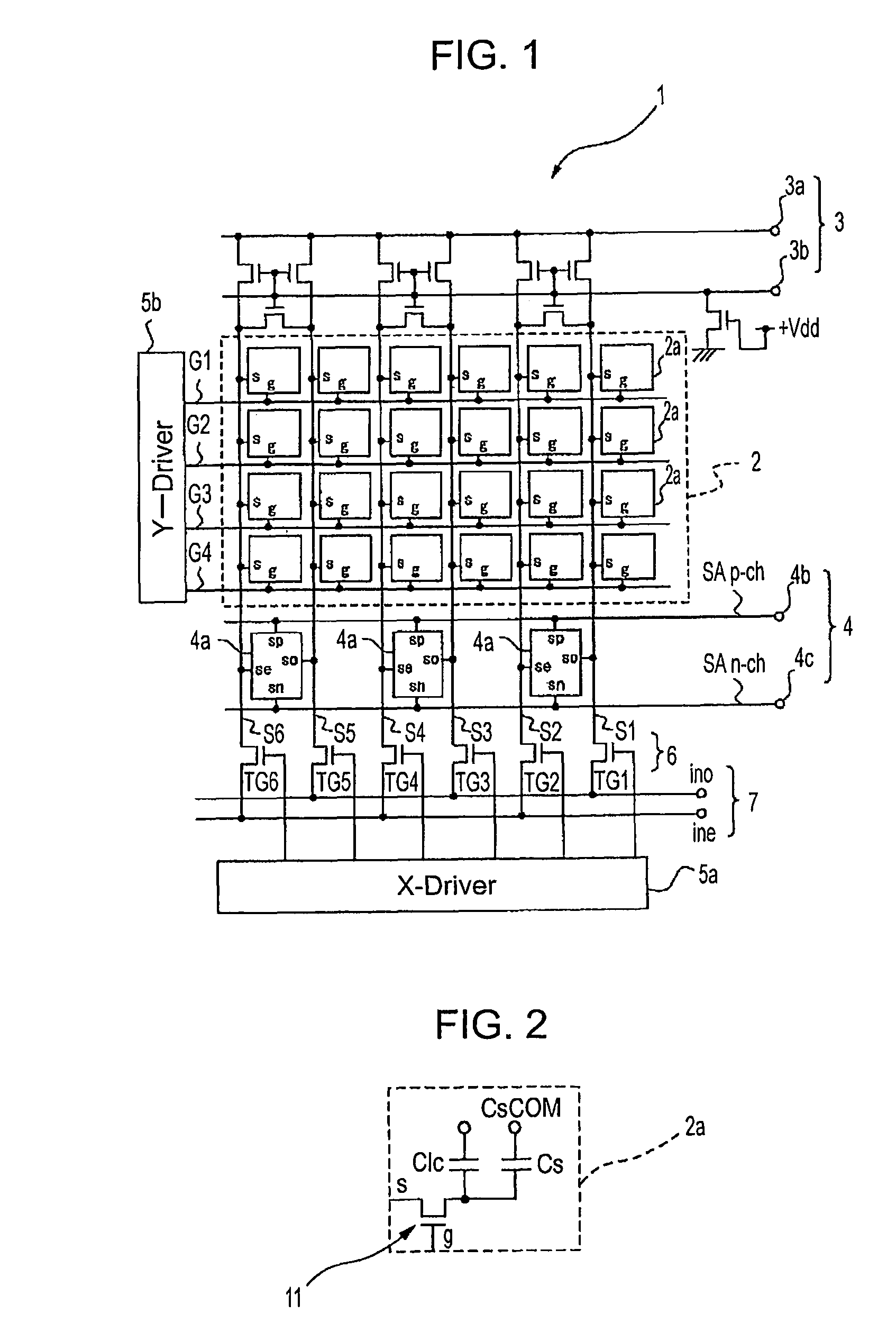
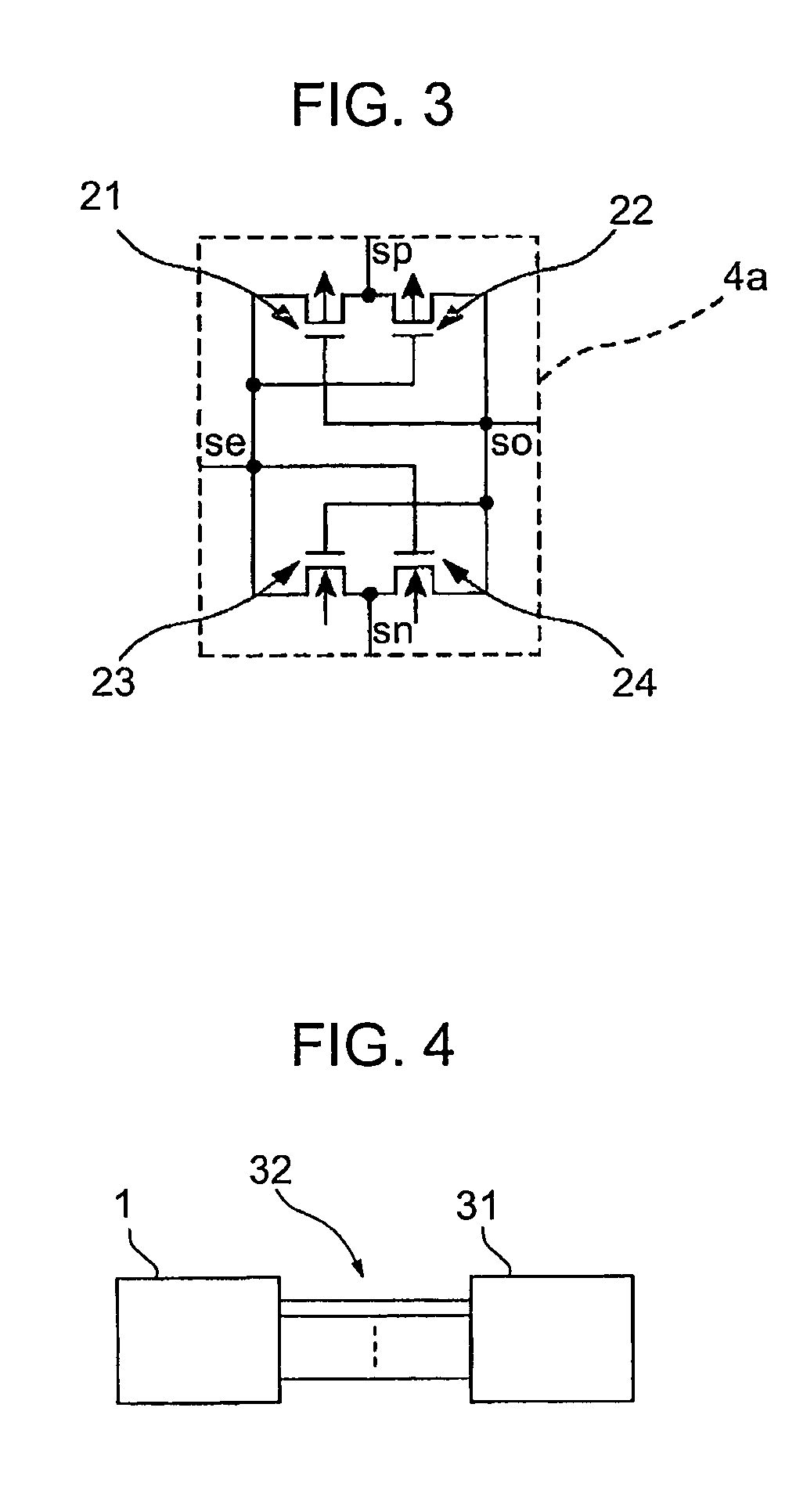
[0090]First of all, FIG. 1 is a circuit diagram of an element substrate of a liquid crystal display device according to a first embodiment of the invention. The element substrate of the liquid crystal display device is an active-matrix type display device substrate. An element substrate 1 includes a display element array portion 2, a pre-charge circuit portion 3 and a display data reading circuit portion 4. The display element array portion 2 serving as a display portion includes multiple pixel cells in a two-dimensional m×n matrix. Here, m and n are both integers. An X-driver portion 5a, a Y-driver portion 5b, a transmission gate portion 6, and an image signal line 7 are further included therein in order to drive multiple pixels 2a aligned in the X-direction (horizontal direction) and Y-direction (vertical direction, of the display element array portion 2. The X-driver portion 5a, Y-driver portion 5b, transmission gate portion 6 and image signal line 7 serve as a data writing unit ...

second embodiment

[0162]Next, a second embodiment of the present invention will be described. FIG. 12 is a circuit diagram of an element substrate of a liquid crystal display device according to the second embodiment of the present invention. In FIG. 12, the same reference numerals are given to the same components as those of the first embodiment, and the description thereof will be omitted herein.

[0163]An element substrate 1B of the liquid crystal display device according to this embodiment also includes the display element array portion 2, the display data reading circuit portion 4, the X-driver portion 5a, the Y-driver portion 5b (not shown in FIG. 12) the transmission gate portion 6, the image signal line 7, and the differential amplifier 10. According to this embodiment, the element substrate 1B further includes a pre-charge circuit portion 13, a connection gate portion 14 and a reference voltage supplying portion 15.

[0164]The pre-charge circuit portion 13 of the second embodiment has a transist...

third embodiment

[0197]Next, a third embodiment of the present invention will be described. FIG. 15 is a circuit diagram of an element substrate of a liquid crystal display device according to the third embodiment of the present invention. In FIG. 15, the same reference numerals are given to the same components as those of the first embodiment, and the description thereof will be omitted herein.

[0198]An element substrate 1C of the liquid crystal display device according to this embodiment also includes the display element array portion 2, the display data reading circuit portion 4, the X-driver portion 5a, the Y-driver portion 5b knot shown in FIG. 15), the transmission gate portion 6, the image signal line 7, and the differential amplifier 10. According to this embodiment, the element substrate 1C further includes a pre-charge circuit portion 16, a connection gate portion 17 and a reference voltage supplying portion 18.

[0199]The pre-charge circuit portion 16 of the third embodiment has a pair of tr...


PUM


Abstract

An electrooptic apparatus substrate and examination method therefor can be provided which can implement an examination without requiring bringing a probe into contact thereto from the outside and with satisfactory measuring accuracy. A substrate 1 of the present invention includes a video line 7 and transmission date portion 6 through multiple switching elements for writing a first potential signal in multiple pixels through a signal line. The substrate 1 further includes a display data reading circuit portion 4 having a differential amplifier 4a for lowering a lower potential and heightening a higher potential and outputting it to the signal line and a transmission gate portion 6 and video line 7 for reading the first potential signal and a reference second potential signal.

Description

TECHNICAL FIELD[0001]The present Invention relates to an electrooptic apparatus substrate and examining method therefor and an electrooptic apparatus and an electronic apparatus. In particular, the present invention relates to an electrooptic apparatus substrate and examining method therefor and electrooptic apparatus and electronic apparatus in which multiple switching devices are provided in multiple pixels.BACKGROUND ART[0002]A display device such as a liquid crystal device has been conventionally and widely used in apparatus such as a cellular phone and a projector. A liquid crystal display device having a TFT (Thin Film Transistor) includes a TFT substrate and a facing substrate, which are pasted to each other, and has liquid crystal sealed between the substrates. In general, the examination for checking whether a manufactured liquid crystal device is performed on the finished product. For example, a predetermined image signal may be input to, projected to and displayed on the ...

Claims


Application Information

Patent Timeline
Patent Type & Authority Patents(United States)
IPC IPC(8): G09G3/36
CPCG09G3/006G09G3/3648G09G2310/0248G09G2330/12
Inventor ISHII, TATSUYAYAMAJI, SHIGEFUMIMIZUGAKI, KOICHI
Owner SEIKO EPSON CORP
Learn More