Supercharge Your Innovation With Domain-Expert AI Agents!

Transistor and display device having the same

a technology of transistor and display device, applied in the field of display devices, can solve the problems of transistor qb>5/b> deterioration, lcd device malfunction, gate driver circuit formation in black matrix region or sealing region, etc., and achieve the effect of reducing the parasitic capacitan

Active Publication Date: 2010-11-30
SAMSUNG DISPLAY CO LTD
View PDF8 Cites 21 Cited by
  • Summary
  • Abstract
  • Description
  • Claims
  • Application Information

AI Technical Summary

Benefits of technology

This configuration effectively minimizes parasitic capacitance, preventing malfunctions in the gate driver circuit and allowing for the use of smaller transistors, which simplifies the manufacturing process and enhances the reliability of the LCD device.

Problems solved by technology

Due to the relatively big size of the transistors Q1 and Q5, forming the gate driver circuit in a black matrix region or a sealing region presents some difficulty.
Furthermore, the hold transistor Q5 may deteriorate, inducing malfunction of the LCD device.

Method used


Image

  • Transistor and display device having the same
  • Transistor and display device having the same
  • Transistor and display device having the same

Examples


Embodiment Construction

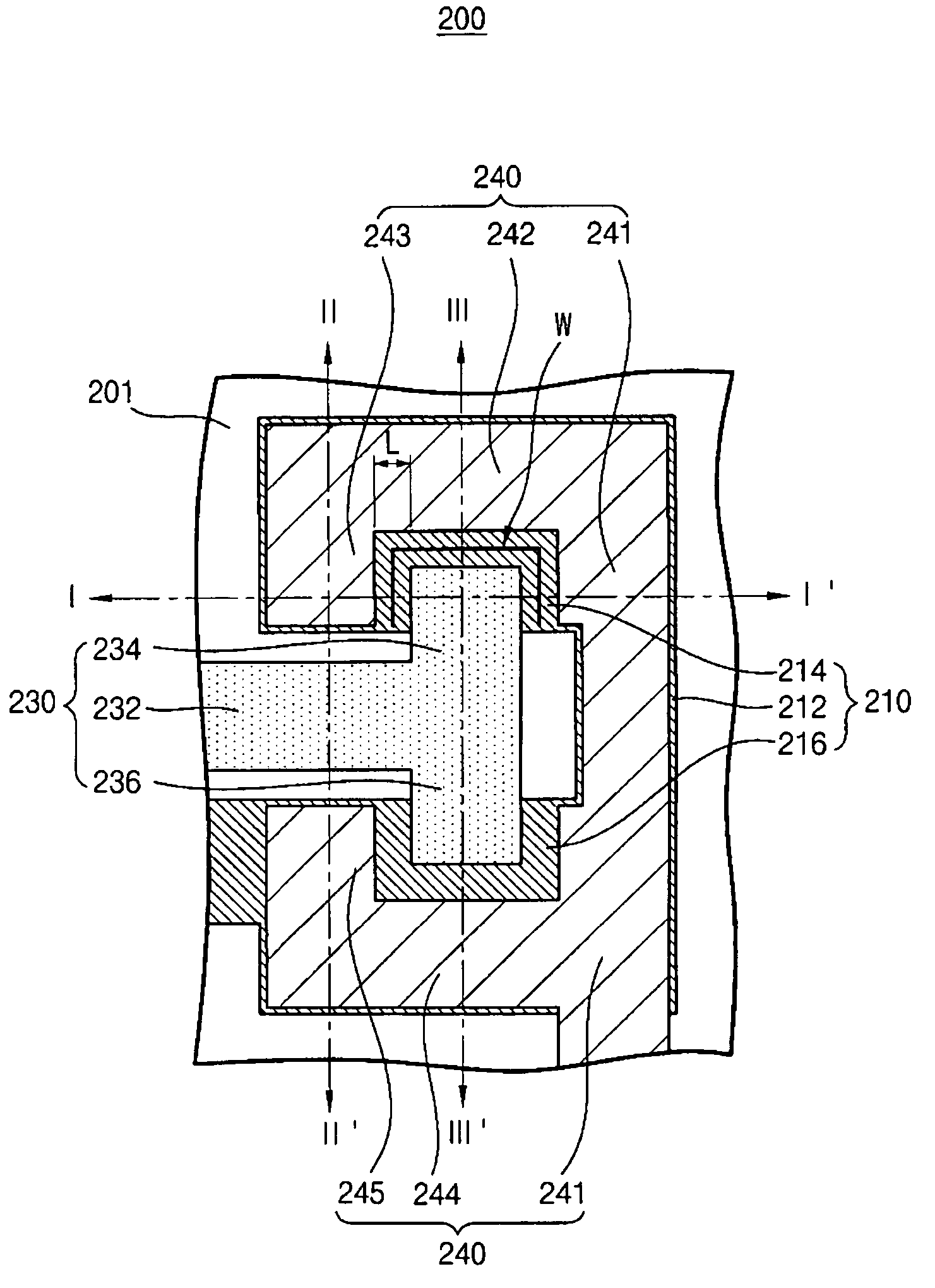
[0066]It should be understood that the exemplary embodiments of the present is invention described below may be varied in many different ways without departing from the inventive principles disclosed herein, and the scope of the present invention is therefore not limited to these particular flowing embodiments. Rather, these embodiments are provided so that this disclosure will be thorough and complete, and will fully convey the concept of the invention to those skilled in the art by way of example and not of limitation.

[0067]Hereinafter, embodiments of the present invention will be described in detail with reference to the accompanied drawings. It is noted that various changes, substitutions and alterations may be made herein without departing from the spirit and scope of the invention as defined by the embodiments described below. The embodiments are examples for showing the spirit of the present invention to a person skilled in the art. In the figures, a thickness of a layer may ...


PUM


Abstract

A transistor includes a control electrode, a first current electrode and a second current electrode. The control electrode includes a body portion, and first and second hand portions protruded from first and second ends of the body portion, respectively. The first current electrode is electrically insulated from the control electrode and disposed over a region between the first and second hand portions of the control electrode. A portion of the first current electrode is overlapped with a portion of the control electrode. The second current electrode is electrically insulated from the control electrode and partially overlapped with the body portion, the first hand portion and the second hand portion of the control electrode. Therefore, parasitic capacitance is reduced.

Description

[0001]This application claims priority to Korean Patent Application No. 2004-72312 filed on Sep. 9, 2004 and all the benefits accruing therefrom under 35 U.S.C. §119, the contents of which are herein incorporated by reference in its entirety.BACKGROUND OF THE INVENTION[0002]1. Field of the Invention[0003]The present invention relates to a device for displaying images. More particularly, the present invention relates to a transistor capable of reducing a parasitic capacitance, and a display device having the transistor.[0004]2. Description of the Related Art[0005]A liquid crystal display (LCD) device employs a gate driver integrated circuit (IC). The gate driver IC is formed, for example, through a tape carrier package (TCP), chip on glass (COG), etc.[0006]Recently, in order to reduce manufacturing cost, a gate-IC-less structure has been developed. According to an LCD device employing the gate IC-less structure, while no gate driver IC is employed, an amorphous silicon thin film tran...

Claims


Application Information

Patent Timeline
Patent Type & Authority Patents(United States)
IPC IPC(8): H01L33/16
CPCH01L27/12H01L29/41733H01L29/42384H01L29/78618H01L29/78669H01L29/78696H01L27/124G02F1/136
Inventor PARK, HAENG-WONMOON, SEUNG-HWANKANG, NAM-SOOLEE, YONG-SOONLEE, BACK-WON
Owner SAMSUNG DISPLAY CO LTD
Features
  • R&D
  • Intellectual Property
  • Life Sciences
  • Materials
  • Tech Scout
  • Unparalleled Data Quality
  • Higher Quality Content
  • 60% Fewer Hallucinations
Learn More