

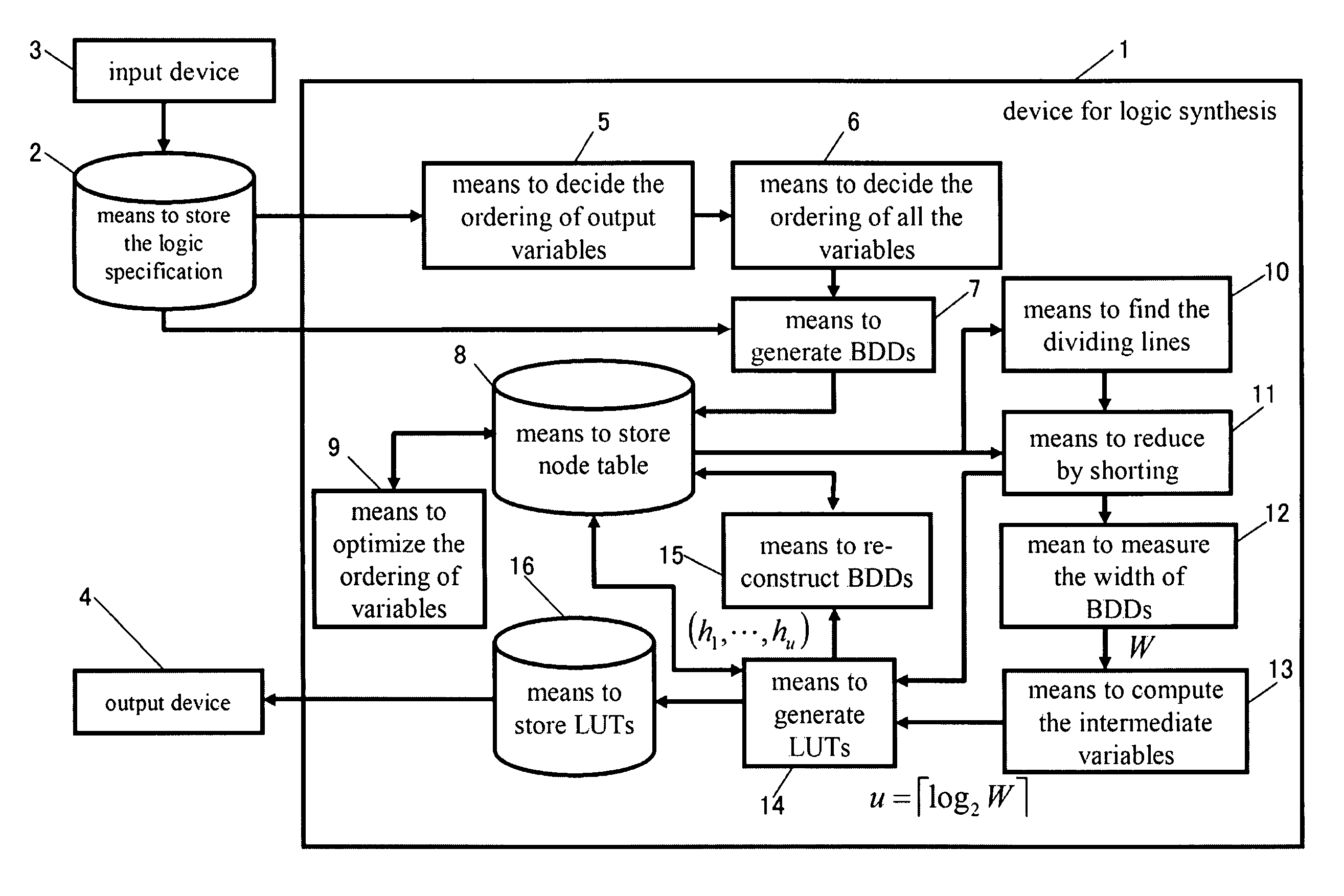
Device for reducing the width of graph and a method to reduce the width of graph, and a device for logic synthesis and a method for logic synthesis
a graph and graph technology, applied in the field of graph and graph width reduction, can solve the problems of difficult design of lut networks or lut cascades with intermediate outputs, inapplicability, etc., and achieve the effect of reducing the width of graphs and reducing the redundancy of lut networks and lut cascades
- Summary
- Abstract
- Description
- Claims
- Application Information
AI Technical Summary
Benefits of technology
Problems solved by technology
Method used
Image

Examples
example 1
[0123]Table 1 shows a decomposition chart of a 4-input 1-output incompletely specified function. Since all the column patterns are different, the column multiplicity μ is 4.[0124][End of Example]
[0125]
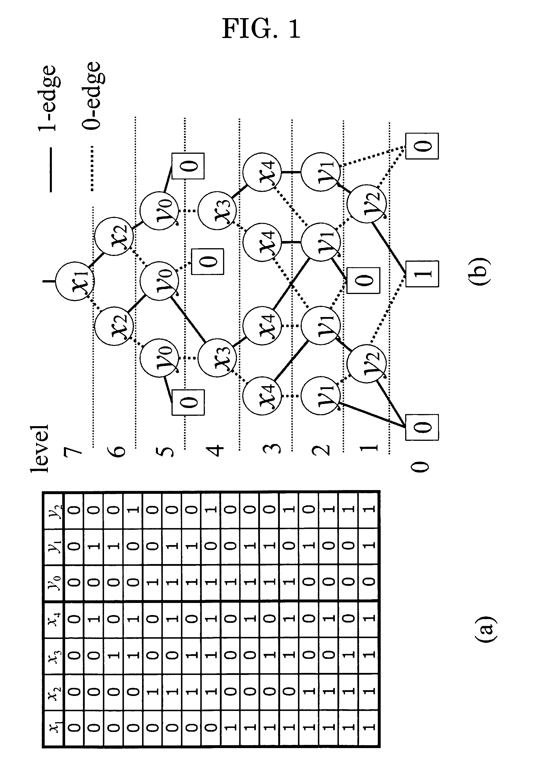
TABLE 1X1 = {x1, x2}00011011X2 = {x3, x4}0000d10111dd10d10d110d00Φ1Φ2Φ3Φ4
[Definition 7] (ON Function, OFF Function, and DC Function)
[0126]The sets of X that satisfy ƒ(X)=0, 1, d, are the OFF set, the ON set, and the DC set, respectively. They are represented by ƒ1(0), ƒ1(1), and ƒ1(d), respectively. Let ƒ(X) be an incompletely specified function of logic variable X(εBn). The OFF function is the function where all the elements in the OFF set ƒ1(0) are mapped to 1, and for other elements are mapped to 0, and is denoted by ƒ—0.
[Equation 1]
[0127]f_0(X)={1(X∈f-1(0))0(otherwise)(1)
[0128]The ON function is the function where all the elements in the ON set ƒ1(1) are mapped to 1, and for other elements are mapped to 0, and is denoted by ƒ—1.
[Equation 2]
[0129]f_1(X)={1(X∈f-1(1))0(otherwise...
example 2
[0147]Consider the 4-input 2-output incompletely specified function shown in Table 2.
[0148]
TABLE 2x1x2x3x4f0f10000d10001d10010000011000100dd0101dd01101001111110000110010110101010111011001d11011d1110d01111d1From Table 2, the OFF function, the ON function, and the DC function are represented as follows:
[0149]From Table 2, the OFF function, the ON function, and the DC function are represented as follows:
[Equation 11]
ƒ0—0= x1x2x3 V x1x2x3
ƒ0—1= x1x2x3 V x1x2x3 V x1x2x3
ƒ0—d= x1x3 V x1x2x3
ƒ1—0= x1x2x3 V x1x2x3 V x2x3x4
ƒ1—1= x2x3 V x2x3x4
ƒ1—d=x2x3 (11)
[0150]Thus, the characteristic function of this function is given as follows:
[Equation 12]
χ={ y0( x1 x2x3 V x1 x2 x3)V y0( x1x2x3 V x1 x2x3 V x1x2 x3)V ( x1 x3 V x1x2x3)}·{ y1( x1 x2x3 V x1 x2x3 V x2x3 x4)V y1( x2 x3 V x2x3x4)V (x2 x3)} (12)[0151][End of Example]
[Definition 10] (Binary Decision Diagram for Characteristic Function)
[0152]The Binary Decision Diagram for Characteristic Function (BDD_for_CF) for a multiple-output logic funct...
example 3
[0154]FIG. 1(b) is the BDD_for_CF that represents the multiple-output logic function in the truth table of FIG. 1(a). Where, a circle denotes a variable node, while a square denotes a terminal node that shows the value of the characteristic function.[0155][End of Example]
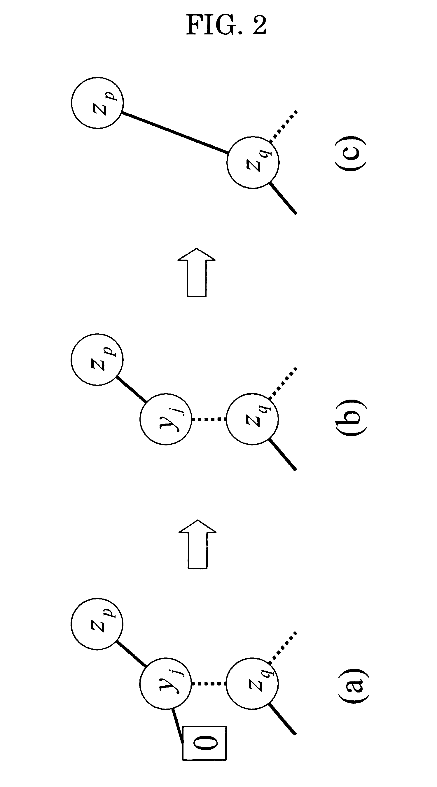
[Definition 11] (Deletion by Shorting)
[0156]In a BDD_for_CF, among the edges that go out from the the nodes yj(εY) for the outputs, remove the edges that are incident to the constant 0, and from the parent node of yj, connect direct by an edge to the child node of yj that is non-constant 0 node. Apply this operation to all the nodes that represent yj. This operation is the removal of the output variable yi by shorting.[0157][End of Definition]
[0158]We will explain the deletion by shorting operation by using FIG. 2. As shown in FIG. 2(a), consider the node representing the output yj(εY). Let zp be the parent node of yj, and zq be a child node of yj. First, delete the node that is connected to the constant 0 terminal ...
PUM
 Abstract
Description
Claims
Application Information