Hologram and method of manufacturing an optical element using a hologram

a manufacturing method and optical element technology, applied in the field of holograms, can solve the problems of insufficient accuracy in some applications of conventional methods of testing and manufacturing aspherical optical surfaces using holograms, and achieve the effect of high quality blaz

Inactive Publication Date: 2010-12-07
CARL ZEISS SMT GMBH
View PDF19 Cites 10 Cited by
  • Summary
  • Abstract
  • Description
  • Claims
  • Application Information

AI Technical Summary

Benefits of technology

[0012]Thus, it is an object of the present invention to provide a method of testing and manufacturing an optical element having an aspherical surface of a relatively high accuracy.
[0042]Other embodiments of the present invention provide a hologram comprising a substrate and a grating provided thereon, wherein the grating comprises a first region in which a grating pitch is low, and a second region, in which the grating pitch is high, i.e. grating forming structures in the second region are repetitive in a greater length scale than in the first region. The grating forming structures in the second region provide a higher quality blaze than the grating forming structures in the first region. This is achieved by including a higher number of path length providing elements in the grating forming structures of the second region as compared to those of the first region.

Problems solved by technology

It has been found that the conventional methods of testing and manufacturing aspherical optical surfaces using a hologram have an insufficient accuracy in some applications.

Method used


Image

  • Hologram and method of manufacturing an optical element using a hologram
  • Hologram and method of manufacturing an optical element using a hologram
  • Hologram and method of manufacturing an optical element using a hologram

Examples


Embodiment Construction

[0060]In the exemplary embodiments described below, components that are alike in function and structure are designated as far as possible by alike reference numerals. Therefore, to understand the features of the individual components of a specific embodiment, the descriptions of other embodiments and of the summary of the invention should be referred to.

[0061]The exemplary embodiments of methods described below involve interferometrically taking measurements of wavefronts generated by an interaction of an incident beam of measuring light provided by an interferometer apparatus with a surface to be measured. Plural conventional interferometric methods may be used as a basis for taking such measurements. Examples of such interferometric methods are disclosed in e.g. U.S. Pat. No. 5,361,312, U.S. Pat. No. 5,982,490 and US 2002 / 0063867 A1. The entire contents of these patents and publications are incorporated herein by reference.

[0062]For illustrating the particularities of embodiments ...


PUM


Abstract

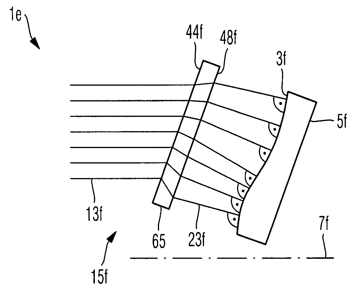
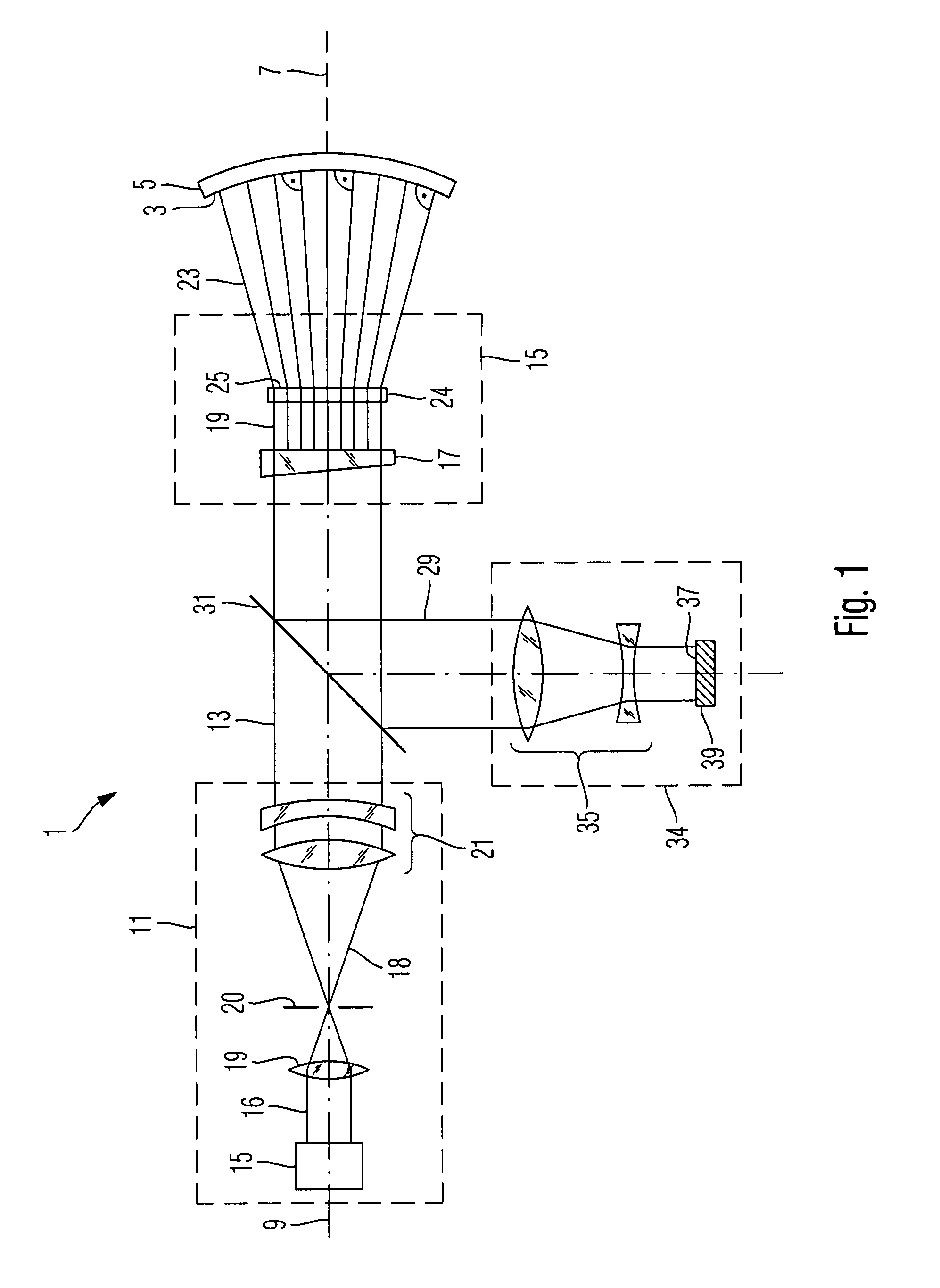
A method of manufacturing an optical element (5) comprises testing an optical surface (3) of the optical element, using an interferometer 1a directing measuring light (23a) onto the optical surface wherein the measuring light traverses two successive holograms (44, 48) disposed in the beam path of the measuring light upstream of the optical surface.

Description

CROSS REFERENCE TO RELATED APPLICATIONS[0001]This application is a National Stage application of International Application No. PCT / EP2006 / 000518, filed Jan. 20, 2006, which designates the United States and was published in English, and which claims the benefit of U.S. Provisional Application No. 60 / 645,710, filed Jan. 20, 2005. These applications, in their entirety, are incorporated herein by reference.BACKGROUND OF THE INVENTION[0002]1. Field of the Invention[0003]The present invention relates to a method of manufacturing an optical element. In particular, the invention relates to a method of manufacturing an optical element having an aspherical shape.[0004]2. Brief Description of Related Art[0005]The optical element having the optical surface is, for example, an optical component such as an optical lens or an optical mirror used in optical systems, such as telescopes used in astronomy, and systems used for imaging structures, such as structures formed on a mask or reticle, onto a ...

Claims


Application Information

Patent Timeline
Patent Type & Authority Patents(United States)
IPC IPC(8): G02B3/02
CPCG01B9/021G01B11/2441G01B9/02039
Inventor HETZLER, JOCHENBEDER, SUSANNEFELDMANN, HEIKO
Owner CARL ZEISS SMT GMBH
Why Eureka
Try Eureka