Two-dimensional photonic crystal

a photonic crystal and two-dimensional technology, applied in the field of two-dimensional photonic crystals, can solve the problems of document 1 not allowing the ff value to be equal or larger than 0.5, deteriorating the light propagation efficiency, etc., and achieve the effect of convenient manufacturing

Inactive Publication Date: 2010-12-14
KYOTO UNIV
View PDF32 Cites 11 Cited by
  • Summary
  • Abstract
  • Description
  • Claims
  • Application Information

AI Technical Summary

Benefits of technology

[0016]According to the present invention, the two-dimensional photonic crystal is created by cyclically arranging modified refractive index areas, which have the same shape, in a slab-shaped body. To create the modified refractive index area, a tangible member whose refractive index differs from that of the body may be embedded into the body. However, it is preferable to make it consisting of air (i.e. a hole) because this design provides a larger difference in refractive index and is easier to manufacture.
[0018]The polygonal shape makes the two-dimensional structure of the crystal less symmetrical than the circular shape. This leads to the creation of two PBGs for the TE-polarized light and the TM-polarized light. The polygonal shape can be appropriately selected so that the two PBGs have a common band and thereby create an absolute PBG. Examples of the polygon include an equilateral triangle, a square and an equilateral hexagon.
[0019]According to the present invention, the corners of the polygon are removed so as to ensure an adequate width of the connecting portion of the body between each corner of the modified refractive index area and that of the neighboring modified refractive index area. This design enables the modified refractive index area, excluding the corner, to be enlarged in order to increase the total area of the modified refractive index areas and thereby obtain a large FF value, while maintaining the two-dimensional photonic crystal at a practically required strength level. Therefore, it is possible to widen the absolute PBG and thereby provide a broader wavelength band available for an optical element or other device than in the case where corners remain. For example, if the plane shape is an equilateral triangle, the conventional FF value theoretically has an upper limit of 0.5, which should be practically 0.45 or lower to ensure an adequate strength of the crystal. In contrast, the FF value in the present invention can be equal to or larger than 0.45, which may be even 0.5 or larger.
[0021]In the present invention, the basic shape of the original polygon must be recognizable even after the corners are removed. For example, suppose that each corner of a triangle is cut along a straight line. If the cutting line is one-third the length of one side, the resultant shape is an equilateral hexagon, so that the basic shape of the equilateral triangle is lost. Therefore, in the present example, the cutting line should be equal to or shorter than one-third the length of one side. In contrast, cutting each corner along an arc leaves the basic shape of the polygon recognizable. This method allows the removed portion of the corner to be larger than in the straight-cutting approach.
[0022]In some cases, the modified refractive index areas do not create any common band shared by both the PBG for the TE-polarized light and that for the TM-polarized light. That is, they may not create an absolute PBG even if their shape is polygonal. An example is the modified refractive index areas having a square shape and arranged in a square lattice pattern. In this example, the absolute PBG cannot be created because no PBG opens for the TM-polarized light. However, a PBG opens for the TE-polarized light. Therefore, this crystal structure can be used as a polarization-dependent device that is effective for only the TE-polarized light. If square holes are arranged in a square lattice pattern, the shortest distance between the neighboring holes is from one side to another, as opposed to the case of triangular holes whose shortest distance is from one corner to another. Even in such a case, the present invention is still effective in that the holes can be easily manufactured.

Problems solved by technology

However, since it has no PBG created for the TM-polarized light, the crystal body allows the TM-polarized light to freely propagate through it.
Therefore, if a ray of light containing both kinds of polarized light is introduced into the waveguide or resonator consisting of a two-dimensional crystal, one of the two polarized lights leaks from the waveguide or resonator into the body, which deteriorates the light-propagating efficiency.
Practically, however, the construction in Non-Patent Document 1 does not allow the FF value to be equal to or larger than 0.5 because the neighboring holes 12 are in contact with each other when the FF value is 0.5, as shown in FIG. 1(b).
Thus, the construction in Non-Patent Document 1 has limitations relating to the setting range of the absolute PBG and the breadth of the wavelength band available, which depends on the absolute PBG.

Method used


Image

  • Two-dimensional photonic crystal
  • Two-dimensional photonic crystal
  • Two-dimensional photonic crystal

Examples


embodiments

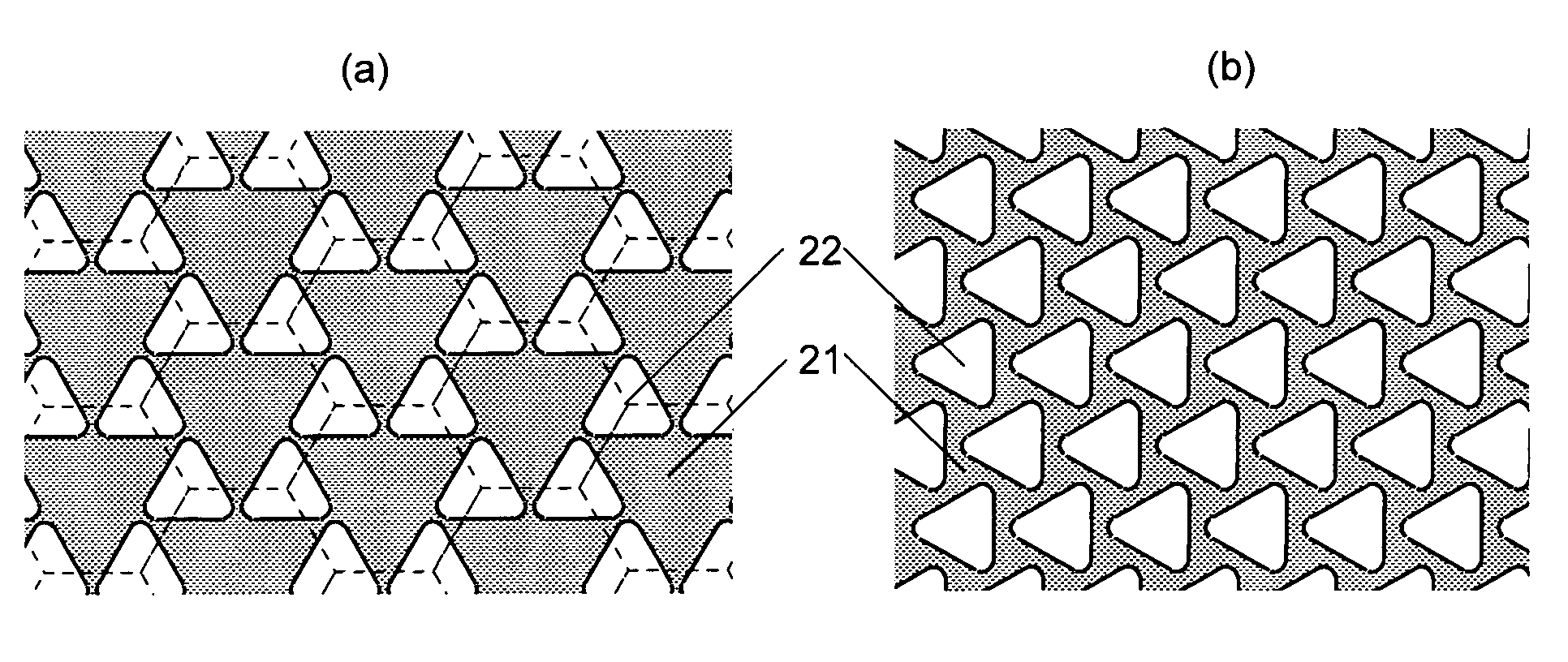
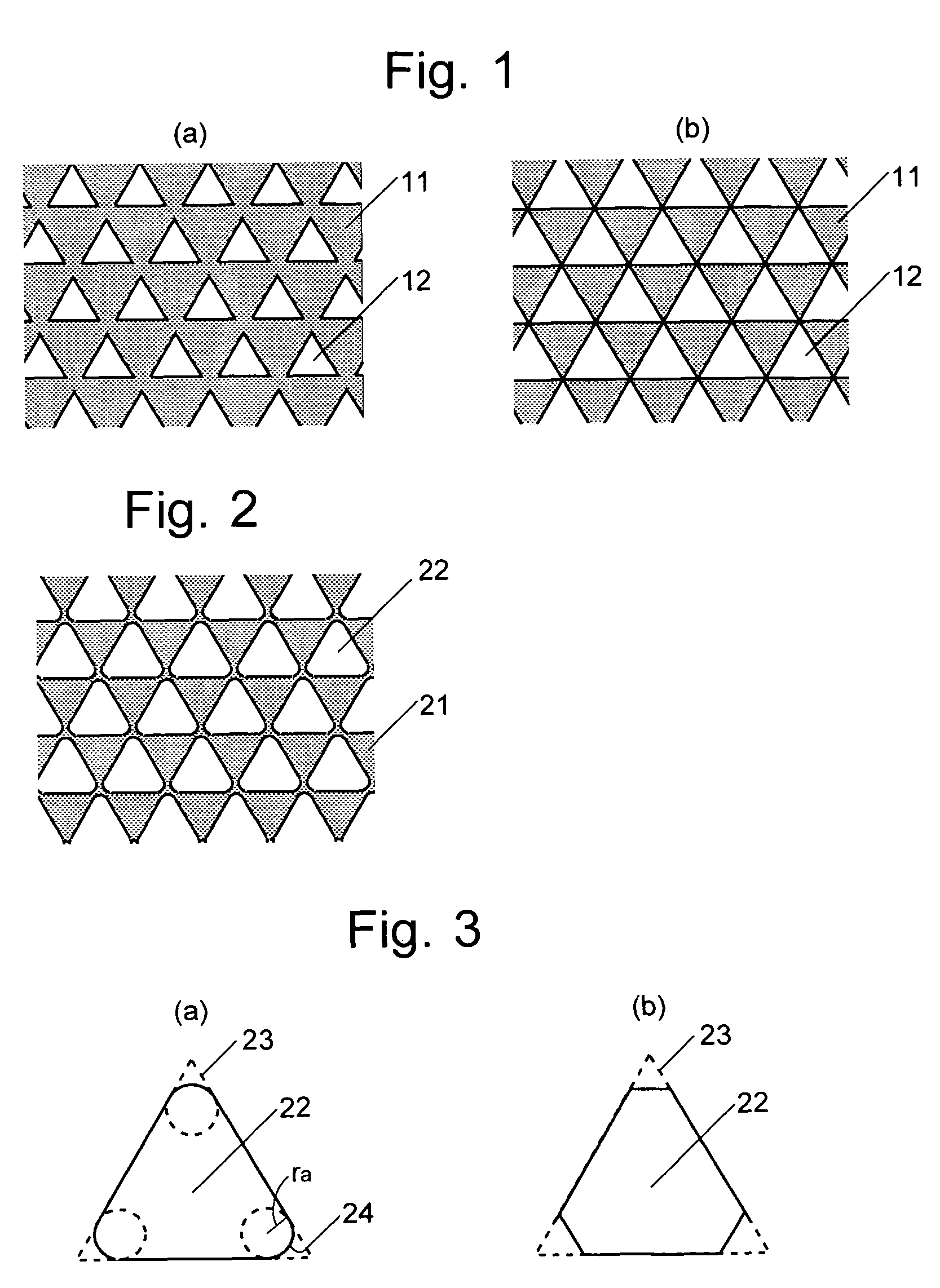
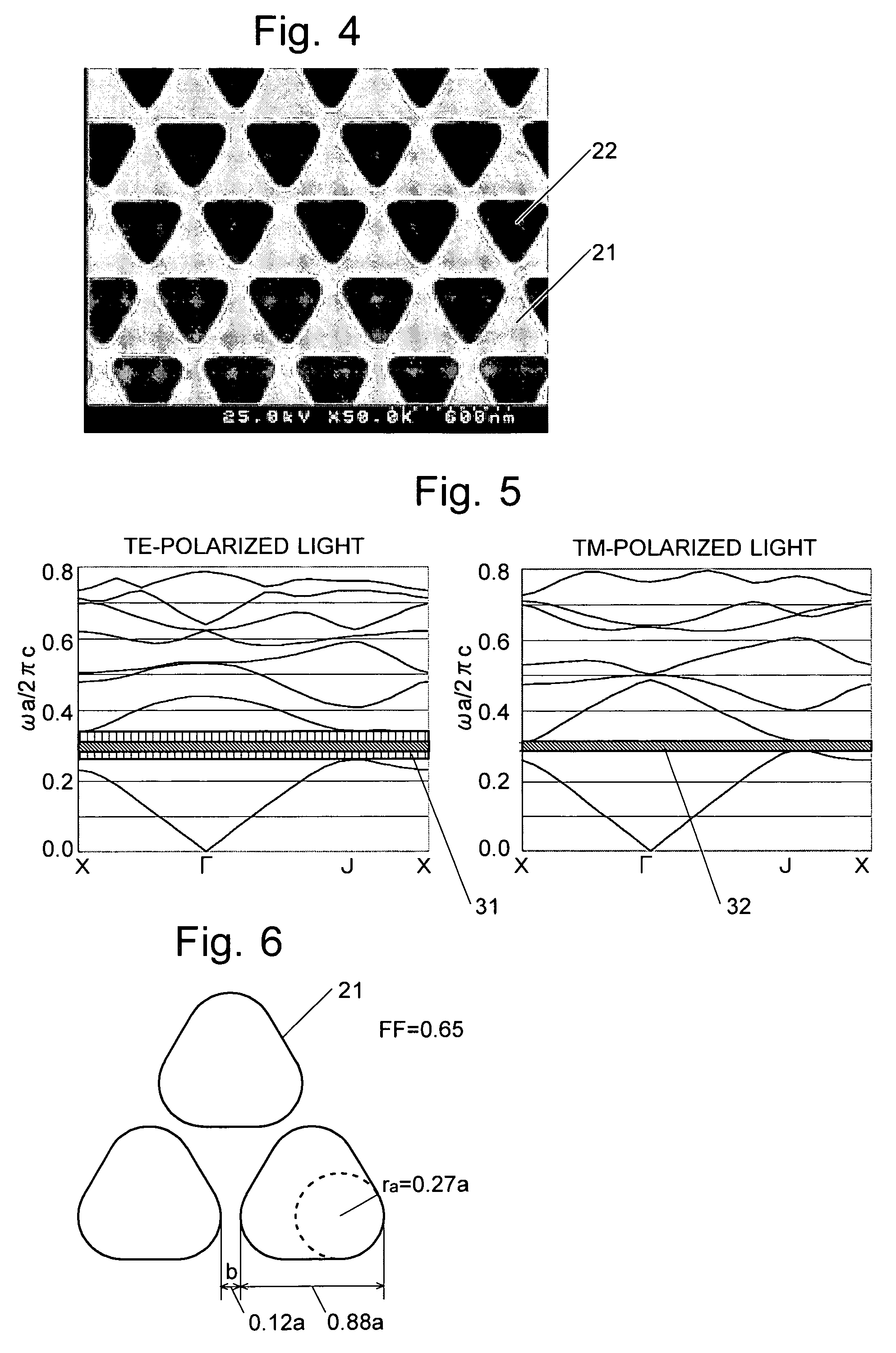
[0040]FIGS. 2 to 4 show an embodiment of the two-dimensional photonic crystal according to the present invention. As shown in FIG. 2, the two-dimensional photonic crystal of the present embodiment consists of a slab-shaped body 21 provided with holes 22 arranged in a triangular lattice pattern. As shown in FIG. 3(a), the basic shape of the holes 22 is an equilateral triangle 23 (broken line) whose corners are each removed along an arc 24 of an inscribed circle having a radius of ra.

[0041]Alternatively, it is possible to remove each corner along a straight line, as shown in FIG. 3(b). However, if an electron-beam drilling process is used to create the hole 22, the arc shape shown in (a) is desirable in that the electron beam leaves a circular edge that can be used as is.

[0042]FIG. 4 shows an electron microscopic image of a two-dimensional photonic crystal actually manufactured, which consists of a slab-shaped silicon body 21 provided with neatly arranged holes 22 having an equilatera...


PUM


Abstract

The present invention provides a two-dimensional photonic crystal in which an absolute photonic band gap (PBG), i.e. a photonic band gap that is effective for both the TE-polarized light and the TM-polarized light within a predetermined wavelength range, is created with an adequate bandwidth. The body 21 is provided with holes 22 arranged in a triangular lattice pattern, where the basic shape of the hole is an equilateral triangle. This shaping and arranging of the holes creates an absolute PBG. Each corner of the equilateral triangle is cut along an arc to leave an adequate distance between the neighboring holes (i.e. an adequate width of the connecting portion of the body). This design makes it possible to enlarge each hole 22 while ensuring an adequate strength of the two-dimensional photonic crystal. This construction creates an absolute PBG having a large width.

Description

TECHNICAL FIELD[0001]The present invention relates to a two-dimensional photonic crystal used as an optical multiplexer / demultiplexer or other kinds of devices in wavelength division multiplexing (WDM) communication or other techniques. It should be noted that the term “light” or “optical” used in this patent application includes electromagnetic waves in general as well as visible light.BACKGROUND ART[0002]Optical communication is a technique that could play a central role in future broadband communications. For widespread use of the optical communication, the optical components used in optical communication systems are required to be higher in performance, smaller in size, and lower in price. Optical communication devices using photonic crystals are one of the leading candidates for the next-generation optical communication components that satisfy the aforementioned requirements.[0003]A photonic crystal is a dielectric object having an artificial cyclic structure. Usually, the cycl...

Claims


Application Information

Patent Timeline
Patent Type & Authority Patents(United States)
IPC IPC(8): G02B6/10G02B6/12G02B1/02G02B6/122G02B6/34
CPCB82Y20/00G02B6/1225G02B6/29325G02B6/2938
Inventor NODA, SUSUMUASANO, TAKASHITAKAYAMA, SEIICHIKITAGAWA, HITOSHI
Owner KYOTO UNIV
Why Eureka
Try Eureka