Unlock instant, AI-driven research and patent intelligence for your innovation.

Printed circuit board design instruction support method and device

Active Publication Date: 2010-12-14
ZUKEN
View PDF6 Cites 6 Cited by
  • Summary
  • Abstract
  • Description
  • Claims
  • Application Information

AI Technical Summary

Benefits of technology

[0070]Since the present invention is constituted as described above, an excellent effect is exerted that the present invention is capable of automatically displaying a design instruction to be referred to in order to correctly perform circuit board design based on a design rule in designing the printed circuit board of electronic equipment.
[0071]Further, since the present invention is constituted as described above, an excellent effect is exerted that the present invention is capable of correctly arranging damping resistances based on a design rule in designing printed circuit board of electronic equipment.
[0072]Further, since the present invention is constituted as described above, an excellent effect is exerted that the present invention is provided with an automatic check function of bypass capacitors including a circuit pattern as EMC measure of a printed circuit board.
[0073]Further, since the present invention is constituted as described above, an excellent effect is exerted that the present invention can be used when displaying the information of parts and wirings, which are referred to in correctly performing circuit board design based on a design rule for each circuit board, as a design instruction, and can be used when displaying a check list for checking whether or not a design is designed as instructed for a printed circuit board.
[0074]Further, since the present invention is constituted as described above, an excellent effect is exerted that the present invention, where the check of drawing can be efficiently executed to improve the work efficiency of printed circuit board design and design quality can be equalized to improve the design quality of printed circuit board, and which are capable of reducing the manufacturing cost of circuit board such as the shortening of a design period and the reduction of the number of making prototypes, becomes possible.
[0075]Further, since the present invention is constituted as described above, an excellent effect is exerted that the present invention, which can be used in verifying whether or not a printed circuit board design of electronic equipment is correctly designed based on a design rule, and in the design verification of a printed circuit board, can simultaneously display areas to be checked both on a circuit diagram and a printed circuit board layout diagram for each circuit part to which the design rule is applied by cooperation between a circuit design system and a printed circuit board design system to shorten check time and lighten labor, becomes possible.

Problems solved by technology

However, instruction was not fully communicated in communication operation by such a design instruction, and further, in the case where the circuit diagram was changed, the names of parts and wirings described on the design instruction needed to be changed in accordance with the change of circuit diagram.
For this reason, in the above-described conventional method, writing and changing work to the design instruction became complicated, and there was a possibility of miswriting the names of parts and wirings, and furthermore, there was the first problem that a problem occurred or quality was deteriorated due to insufficient communication on written instruction.
Further, regarding the design quality of a designed printed circuit board, a design instruction itself depends on designers, so that its quality varies according to the skill of designers, and there was the second problem that instruction contents were affected by instruction designers such that printed circuit board design quality is deteriorated due to human-dependent situation.
Specifically, there are many areas where the damping resistance must be extracted from the circuit diagram visually, and it was difficult to judge by anyone but the designer himself / herself.
Then, in designing printed circuit board, although it is necessary to instruct which resistance is the damping resistance by using the position and the wiring method of damping resistance as a circuit board design instruction, enormous time was required in extracting the damping resistance because no condition existed in extracting the damping resistance.
In short, the design instruction for the damping resistance is necessary in designing printed circuit board and checking printed circuit board, but there was the third problem that enormous time was required in extracting the damping resistance itself.
Furthermore, the number of LSIs to be mounted increases as a circuit size becomes larger, and the increase of LSIs directly connected to the increase of the number of bypass capacitors.
With the increase of the bypass capacitors, there was the fourth problem that much labor and time cost was consumed in recognizing as many as several hundred bypass capacitors, for example, by using a screen of CAD system and a drawing of layout, which was drawn on paper.
It is to be noted that there is a method of applying attribute into the bypass capacitors in designing a circuit, but load in designing becomes heavier and such method was difficult to be realized.
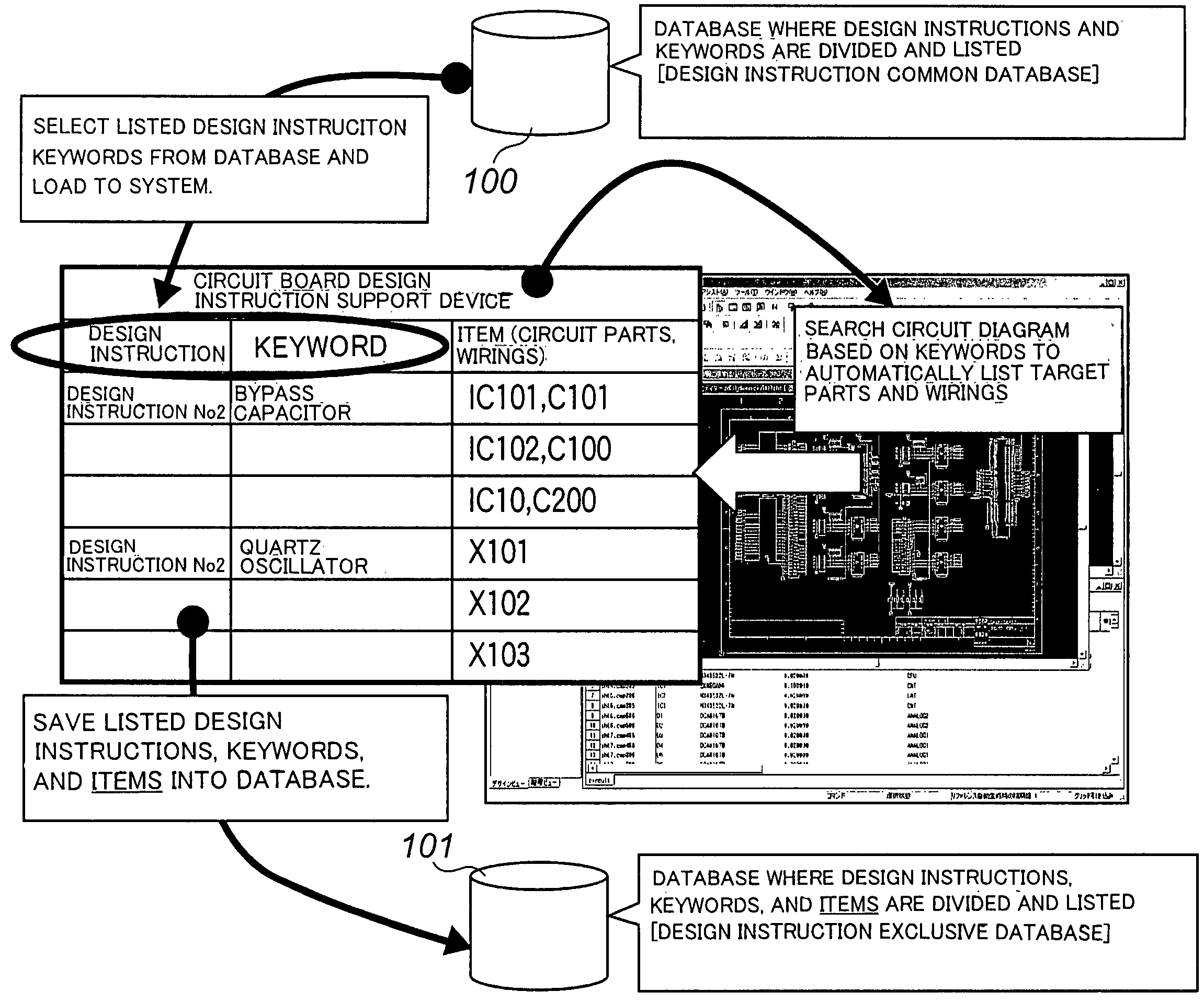
Specifically, design instruction for bypass capacitors is necessary in designing printed circuit board and checking printed circuit board, and there was the fifth problem that enormous time was required in extracting bypass capacitors.
Conventionally, search processing has been done for each item (parts, wiring information, etc.) in extracting the groups, enormous time was required in extracting work in proportion to the article quantity of items and parts quantity, and further, extracted data are inherent to the circuit diagram, so that there was the sixth problem that workload and much time in proportion to items were required such that the same extracting work was necessary in another circuit diagram.
Specifically, because of reasons such as sudden increase of the difficulty level of design caused by digitalization and the difficulty of maintaining the integrity of an entire system by the shortened competitiveness of products or multi-function, the reasons such as the design quality dependent on designers, labor spent in drawing check and corrected instruction is enormous, and shortening the labor has been the key to shorten the lead time of design.
For this reason, there was the seventh problem that the work efficiency deteriorated and enormous labor and cost were required in inspection, confirmation, and drawing check regarding a designed printed circuit board or creating a correction instruction.
Herein, since some design instructions have rules that cannot be expressed in numerical values, there were cases where automatic check using a CAD system could not be performed, and check for such portions had to be done visually.
To use the function, it is necessary to operate both the circuit diagram and the printed circuit board, and furthermore, since there are cases where articles that must be checked are several hundred or more depending on a product, there was the eighth problem that enormous labor and time were required in check.
Specifically, if the contents to be checked are not clearly displayed, there is a possibility that the check contents are misrecognized and accurate check cannot be performed.
There was the ninth problem that the work of performing display control every time to prevent misrecognition depended on the skill of operators and it caused significant loss of time.
Furthermore, even if an instruction is given in designing printed circuit board, such instruction contains contents whose quality cannot be maintained unless the circuit board is designed accompanied by knowledge such as experience and logic.
Conventionally, the designer of printed circuit board has needed to search and read books and materials of corresponding technical information in order to understand the instruction, and there was the tenth problem that the designer of printed circuit board needed to spend enormous time in searching and reading the technical information.

Method used


Image

  • Printed circuit board design instruction support method and device
  • Printed circuit board design instruction support method and device
  • Printed circuit board design instruction support method and device

Examples


Embodiment Construction

[0106]In the following, description will be made in detail for an embodiment example of the a printed circuit board design instruction support method between a circuit design and a printed circuit board design, the printed circuit board instruction support device between a circuit design and a printed circuit board design, the Web system, the program, and the computer-readable recording medium according to the present invention with reference to the attached drawings.

[0107]1. Overall Constitution

[0108]The printed circuit board design instruction support device between a circuit design and a printed circuit board design (hereinafter, simply referred to as “printed circuit board design instruction support device” appropriately) 10 according to the present invention is an integrated system of each system (described later), and the printed circuit board design instruction support device 10 cooperates a circuit design system 12 and a printed circuit board design system 14 as shown in FIG...


PUM


Abstract

There are provided a printed circuit board design instruction support method between a circuit design and a printed circuit board design, a printed circuit board design instruction support device between a circuit design and a printed circuit board design, a Web system, a program, an a computer-readable recording medium which improve the work efficiency of the printed circuit board designing and the quality of the printed circuit board design. By selecting a circuit part to which the design rule is applied, a circuit program and a portion-to-be-checked on the printed circuit board are simultaneously displayed by cooperation between the circuit design system and the printed circuit board design system, thereby reducing the time and labor required for check.

Description

TECHNICAL FIELD[0001]The present invention relates to a printed circuit board design instruction support method between a circuit design and a printed circuit board design, a printed circuit board instruction support device between a circuit design and a printed circuit board design, a Web system, a program, and a computer-readable recording medium, more specifically to a printed circuit board design instruction support method between a circuit design and a printed circuit board design, a printed circuit board instruction support device between a circuit design and a printed circuit board design, a Web system, a program, and a computer-readable recording medium, which are designed to improve the work efficiency of the printed circuit board design and to improve the quality of the printed circuit board design.BACKGROUND TECHNOLOGY[0002]Conventionally, in creating a design instruction to design a printed circuit board on a circuit design step, a circuit designer has been supposed to w...

Claims


Application Information

Patent Timeline
IPC IPC(8): G06F17/50G06G7/62
CPCG06F17/5081G06F30/398
Inventor INAISHI, HIROMICHITANAKA, HIROYUKIFUKUOKA, KEISUKEYAMAWAKI, MASAHIROAJIMINE, ASAKO
Owner ZUKEN
Features
  • R&D
  • Intellectual Property
  • Life Sciences
  • Materials
  • Tech Scout
  • Unparalleled Data Quality
  • Higher Quality Content
  • 60% Fewer Hallucinations
Learn More