Formation of high sheet resistance resistors and high capacitance capacitors by a single polysilicon process

a polysilicon and capacitor technology, applied in capacitors, semiconductor devices, diodes, etc., can solve the problems of increasing the cost of device components, increasing the cost of manufacturing, so as to achieve high capacitance and high sheet resistance

Active Publication Date: 2010-12-21
ALPHA & OMEGA SEMICON LTD
View PDF4 Cites 10 Cited by
  • Summary
  • Abstract
  • Description
  • Claims
  • Application Information

AI Technical Summary

Benefits of technology

[0008]It is therefore an aspect of the present invention to provide a new and improved semiconductor device configuration and manufacturing processes to provide high sheet resistance and high capacitance by implementing a single polysilicon configuration and method such that the limitations and difficulties discussed above can be resolved.

Problems solved by technology

These types of device components become more costly to implement.
The process of manufacture becomes more time consuming and complicated.
Furthermore, the device reliability is also adversely affected due to the more complicate manufacturing processes.
These types of device components become more costly to implement.
The process of manufacture becomes more time consuming and complicated.

Method used


Image

  • Formation of high sheet resistance resistors and high capacitance capacitors by a single polysilicon process
  • Formation of high sheet resistance resistors and high capacitance capacitors by a single polysilicon process
  • Formation of high sheet resistance resistors and high capacitance capacitors by a single polysilicon process

Examples


Embodiment Construction

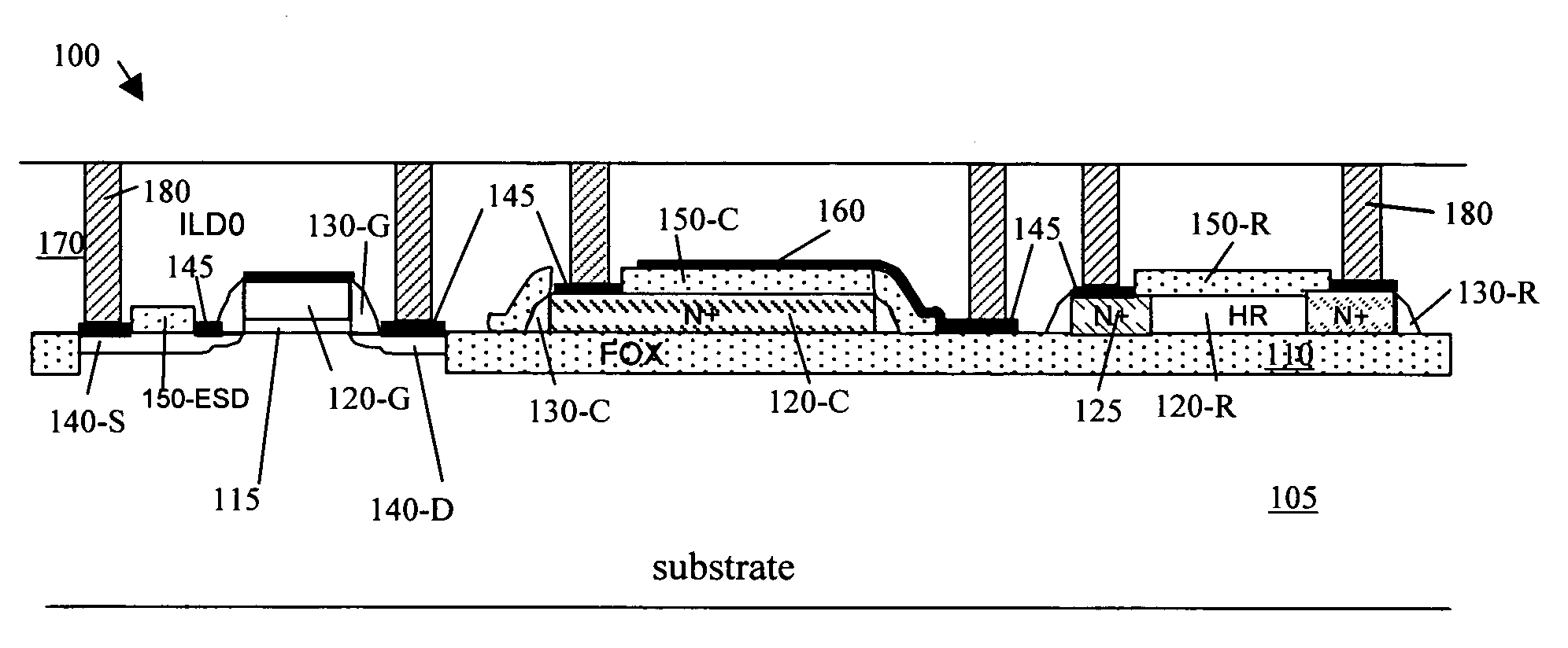
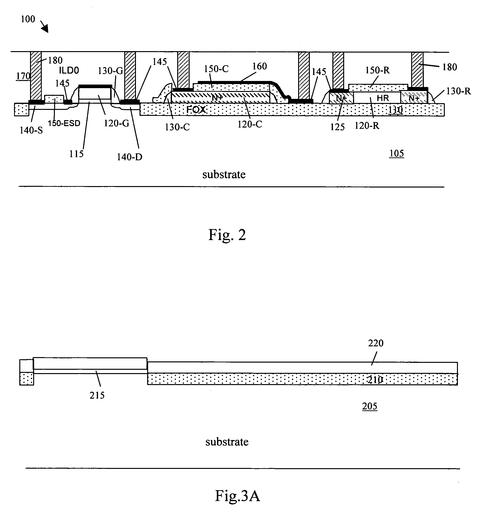
[0016]Referring to FIG. 2 for a cross sectional view of a semiconductor device 100. The semiconductor device 100 is supported on a substrate 105 formed with a field oxide layer 110. The field oxide layer is formed adjacent to a transistor area. The top surface of the field oxide layer 110 is to support resistor and capacitor. On the top surface of the transistor area, a transistor is formed with a polysilicon gate 120-G disposed on top of a gate oxide layer 115 between a source region 140-S and a drain region 140-D. The gate is surround by a spacer layer 130-G. The transistor is further provided with a ESD protection layer 150-ESD formed on top of a N+ or P+ diffusion resistor layer 140-S or 140-D that in turn is connected to a tungsten plug 180 filled in a trench opened through an zero void inter-layer dielectric (ILD0) layer 170.

[0017]A capacitor is supported on the top surface of the field oxide layer 110 that includes a N+ doped polysilicon layer 120-C to function as the bottom ...


PUM


Abstract

A semiconductor device includes a transistor, a capacitor and a resistor wherein the capacitor includes a doped polysilicon layer to function as a bottom conductive layer with a salicide block (SAB) layer as a dielectric layer covered by a Ti / TiN layer as a top conductive layer thus constituting a single polysilicon layer metal-insulator-polysilicon (MIP) structure. While the high sheet rho resistor is also formed on the same single polysilicon layer with differential doping of the polysilicon layer.

Description

BACKGROUND OF THE INVENTION[0001]1. Field of the Invention[0002]The invention relates generally to the semiconductor power devices. More particularly, this invention relates to an improved and novel device configuration and manufacturing process to provide electronic device and resistor with high sheet resistance and capacitor with high capacitance by employing a single polysilicon process.[0003]2. Description of the Prior Art[0004]Conventional processes for manufacturing device component that has resistor with high sheet resistance and capacitor with high capacitance generally apply a double polysilicon process. The processing steps for making double polysilicon components involve multiple masks and additional processing steps. These types of device components become more costly to implement. The process of manufacture becomes more time consuming and complicated. Furthermore, the device reliability is also adversely affected due to the more complicate manufacturing processes. As th...

Claims


Application Information

Patent Timeline
Patent Type & Authority Patents(United States)
IPC IPC(8): H01L29/76
CPCH01L27/0629H01L28/20H01L28/60Y10S438/957
Inventor HU, YONGZHONGTAI, SUNG-SHAN
Owner ALPHA & OMEGA SEMICON LTD
Why Eureka
Try Eureka