Semiconductor device using SOI-substrate

a technology of soi substrate and semiconductor device, which is applied in the direction of semiconductor device, basic electric element, electrical apparatus, etc., can solve the problems of increased leak current, increased performance, and difficulty in improving the performance of a conventional bulk-cmos, so as to increase the resistance to source/drain voltage and increase the allowable electric power

Active Publication Date: 2010-12-28
LAPIS SEMICON CO LTD
View PDF6 Cites 4 Cited by
  • Summary
  • Abstract
  • Description
  • Claims
  • Application Information

AI Technical Summary

Benefits of technology

[0014]Another object of the present invention is to provide an improved semiconductor device and an improved method for fabricating the same, in which an allowable electric power is increased.
[0019]According to the present invention, a depletion layer extends both toward a channel region and a lower part of a drain region, so that a junction area between the drain region and a SOI layer is increased. As a result, a source / drain voltage resistant is increased while keeping fundamental characteristics of FS-SOI. In addition, an allowable electric power is increased.

Problems solved by technology

On the other hand, when the threshold voltage “Vt” of transistors decreases, performance, including the operation speed, would be increased, however, leak current would be increased.
However, since performance of a transistor depends on physical characteristics, including device structure and impurity profile, it is difficult to improve performance of a conventional bulk-CMOS.
As a result, devices are easily damaged or broken with heat.
In addition, according to a FD-SOI, a source / drain voltage resistant is low, so that a power supply voltage may not be determined high; and is not appropriate for a protection device because of a device damage or brokenness.

Method used


Image

  • Semiconductor device using SOI-substrate
  • Semiconductor device using SOI-substrate
  • Semiconductor device using SOI-substrate

Examples


Embodiment Construction

[0028]In the following detailed description of the preferred embodiments, reference is made to the accompanying drawings which form a part hereof, and in which is shown by way of illustration specific preferred embodiments in which the inventions may be practiced. These preferred embodiments are described in sufficient detail to enable those skilled in the art to practice the invention, and it is to be understood that other preferred embodiments may be utilized and that logical, mechanical and electrical changes may be made without departing from the spirit and scope of the present inventions. The following detailed description is, therefore, not to be taken in a limiting sense, and scope of the present inventions is defined only by the appended claims.

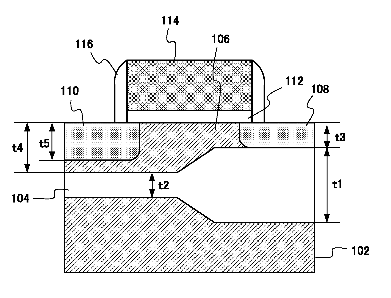
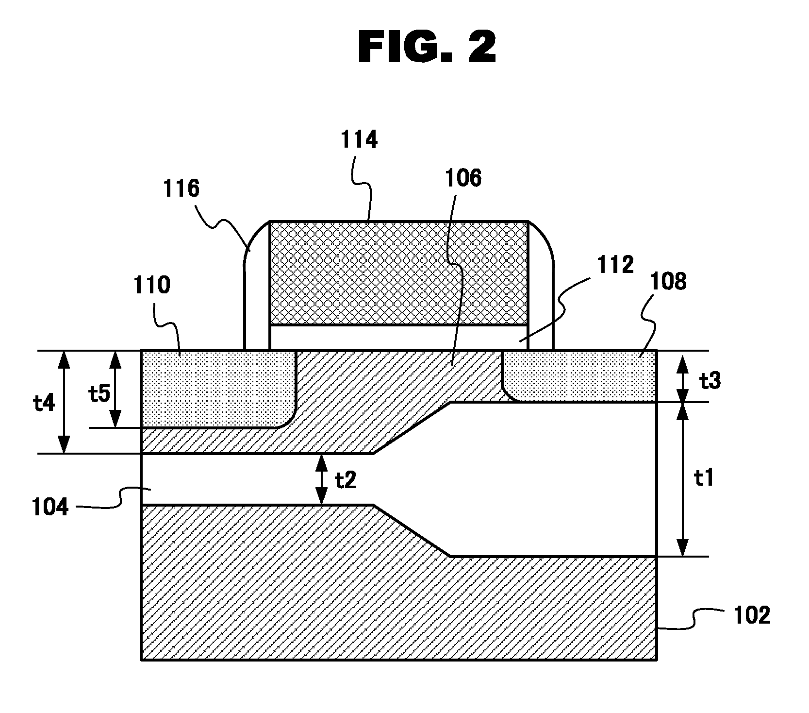
[0029]FIG. 2 is a cross sectional view illustrating a structure of a semiconductor device according to an embodiment of the present invention. A semiconductor device, according to the present embodiment, is fabricated using a SOI subs...


PUM


Abstract

According to a feature of the present invention, a semiconductor device includes a SOI substrate, including a semiconductor substrate; an insulating layer formed on the semiconductor substrate and a silicon layer formed on the insulating layer. A drain region and a source region are formed in the silicon layer so that the source region is in contact with the insulating layer but the drain region is not in contact with the insulating layer.

Description

CROSS REFERENCE TO RELATED APPLICATION[0001]This application claims the priority of Application No. 2007-324136, filed Dec. 17, 2007 in Japan, the subject matter of which is incorporated herein by reference.TECHNICAL FIELD OF THE INVENTION[0002]The present invention relates to a semiconductor device using a SOI substrate and a method for fabricating the same. In particular, the present invention relates to a high voltage device, having improved characteristics of source / drain voltage resistant, and a method for fabricating the same.BACKGROUND OF THE INVENTION[0003]In general, performance and efficiency of a LSI depends on performance and efficiency, including power consumption, of transistors. When the threshold voltage “Vt” of transistors increases, leak current would be reduced and power consumption would improve. However, performance, including the operation speed, would be decreased, under a condition of constant voltage supply. On the other hand, when the threshold voltage “Vt”...

Claims


Application Information

Patent Timeline
Patent Type & Authority Patents(United States)
IPC IPC(8): H01L21/00H01L21/84
CPCH01L29/78603H01L29/78618H01L29/78654
Inventor HAYASHI, HIROKAZU
Owner LAPIS SEMICON CO LTD
Why Eureka
Try Eureka